MP7643AN 查看數據表(PDF) - Exar Corporation
零件编号
产品描述 (功能)
比赛名单
MP7643AN Datasheet PDF : 12 Pages
| |||
MP7643
THEORY OF OPERATION
The MP7643 is a 4-channel multiplying D/A converter that in-
corporates a novel open loop architecture invented by MPS.
The design produces the wider bandwidth, faster settling time,
more constant group delay, and a lower noise operation
compared to the conventional R-2R based architectures. This
device is particularly useful in applications where analog multi-
pliers are used to perform the gain adjustment function for high
frequency analog signal conditioning. Analog multipliers pro-
duce higher noise and offset. This design allows for digital con-
trol of gain with constant and very low noise from the low gain
through high gain ranges of operation.
Linearity Characteristics
Each DAC achieves DNL +0.5 LSB (typ), INL +1 LSB
(typ), and gain error +1.5%. Since all 4 channel D/A convert-
ers are fabricated on the same IC, the linearity matching and
gain matching of +0.5% (typ) is achieved.
AC and Transient Settling Characteristics
The novel subranging architecture delivers a 15 MHz (typ.)
–3 dB bandwidth. With all codes = 1 and a 1.6 V step impulse at
VREF(1-4), the analog output settles to 8 bits of accuracy in typi-
cally 150 ns (with RL = 5k to VEE). Also with VREF = 3 V or –3 V
and a FS to ZS or ZS to FS code change, the respective analog
output settles to 8 bits typically in 300 ns. Note that the AC per-
formance specifications also match between all 4 channels.
The above AC and transient performance is achieved with each
channel consuming only 20 mW (typ.) with either 5 V or 0 V to
10 V supplies.
Digital Interface
The MP7643 allows direct interface to most microprocessor
buses without additional I/O circuitry. Figure 1. and Figure 2.
describe the operation, specification and interface characteris-
tics of the logic port.
The address bits A0 and A1 determine which D/A channel is
selected. When LD input is low the respective latch of the D/A is
enabled (digital input data becomes transparent to the latch and
the selected DAC channel), and digital data is loaded into the se-
lected DAC.
Power Supplies and Voltage Reference DC Voltage
Ranges
For the single supply operation, VCC = +10 V, VDD = +5 V, and
VEE = GND = 0 V. The VOUT 1-4 and VREF 1-4 range would be
VCC –1.8 V (10 – 1.8 = 8.2 V) to VEE +1.5 V (0 + 1.5 = 1.5 V).
VREFN is the equivalent of AGND for this DAC. In this mode
VREFN can be set at (VCC + VEE)/2 = (10 + 0)/2 = 5 V. VREFN DC
range can, however, be set from VEE +1.5 = 1.5 V to VCC – 1.5 =
8.2 V. Refer to Table 2. for the relationship equations.
For the dual supply operation, VCC = +5, VDD = +5, and VEE =
–5 V. The VOUT 1-4 and VREF 1-4 range would be VCC –1.8 V (5
V –1.8 = 3.2 V) to VEE +1.5 V (–5 + 1.5 = –3.5 V). In this mode
VREFN can be set to (VCC + VEE)/2 = (5 – 5)/2 = 0 V. However,
VREFN DC range can be set from VEE +1.5 V = 3.5 V to VCC –1.8
= +3.2 V. Refer to Table 2. for the relationship equations.
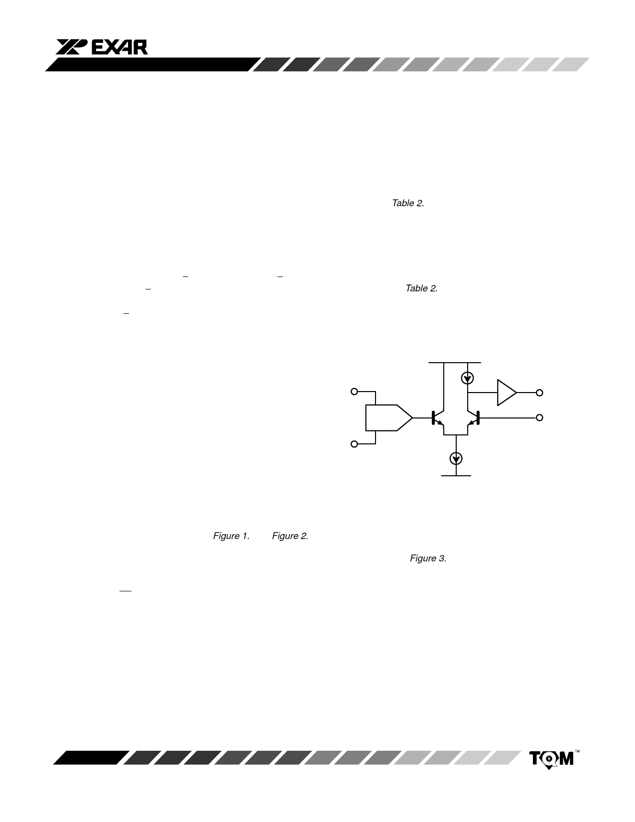
About the INV Input and its DC Voltage Range
VREF 1-4
DAC
VCC
+1
Q2 Q1
VOUT 1-4
INV 1-4
VREFN
I1
VEE
Figure 3. Simplified Block Diagram
As noted in the specification table, the max DC value of the
INV input pin is VO. Figure 3. shows a simplified block diagram
of the internal circuitry around INV. If VINV exceeds VO, Q1 will
saturate and the amp and consequently the DAC becomes non-
functional.
The min DC range of INV is limited to Vbe (Q1) and VCE (sat)
of I1. Therefore, INV (min-DC) = VEE +1 V.
Rev. 1.00
7
Share Link: 