MSM7540 查看數據表(PDF) - Oki Electric Industry
零件编号
产品描述 (功能)
比赛名单
MSM7540 Datasheet PDF : 15 Pages
| |||
¡ Semiconductor
MSM7540/7560
PIN AND FUNCTIONAL DESCRIPTIONS
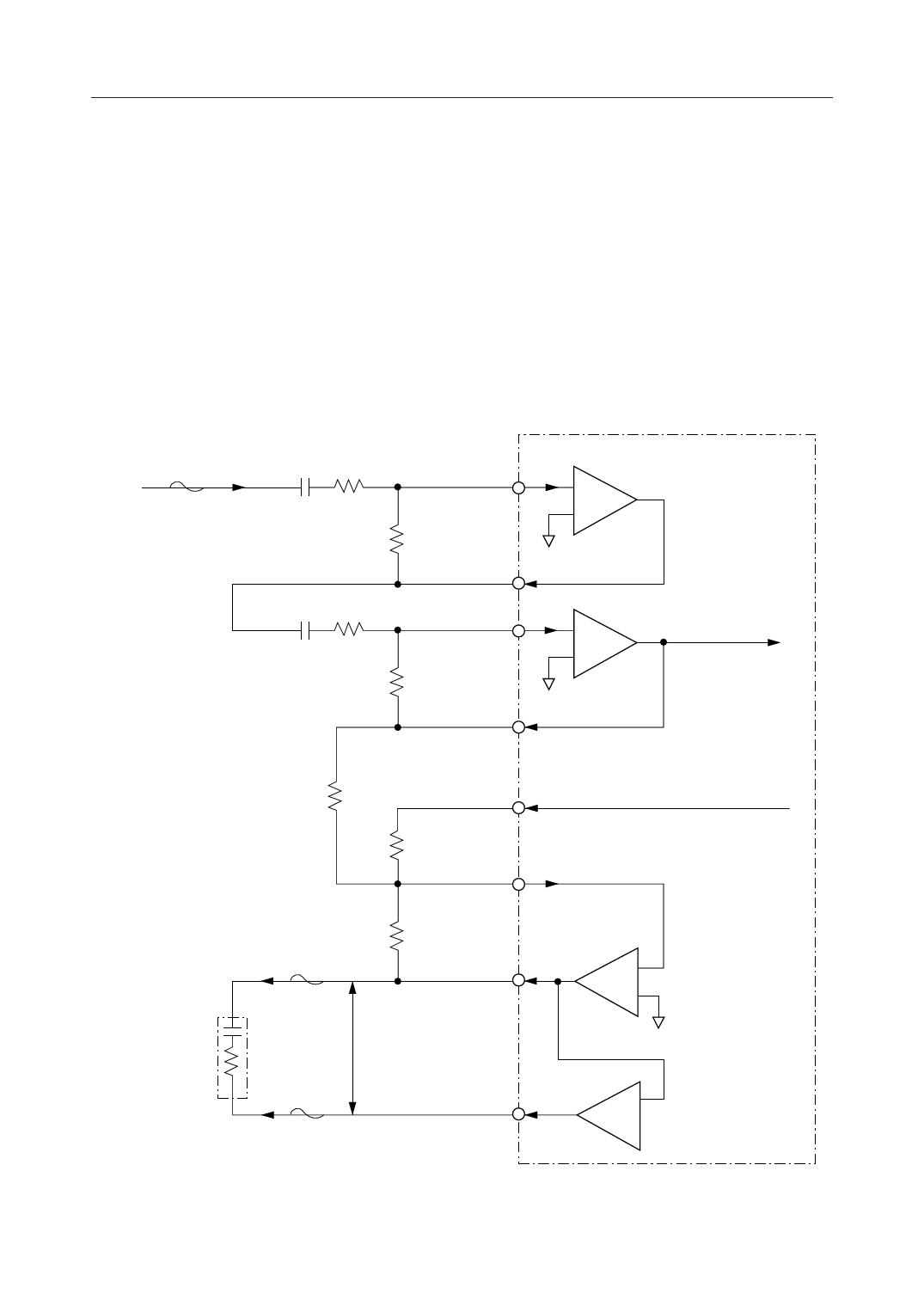
AIN1, AIN2, GSX1, GSX2
Transmit analog inputs and the output for transmit gain adjustment.
AIN1 (AIN2) connects to the inverting input of the internal transmit amplifier. GSX1 (GSX2)
connects to the internal transmit amplifier output. Refer to Fig. 1 for gain adjustment.
VFRO, AOUT+, AOUT–, PWI
Receive analog output and the output for receive gain adjustment.
VFRO is the receive filter output. AOUT+ and AOUT– are differential analog signal outputs
which can directly drive ZL = 350 W + 120 nF. Refer to Fig. 1 for gain adjustment.
Analog Input
C1 R1
R2
C2 R3
R4
Transmit Gain:
= (R2/R1) ¥ (R4/R3)
RS*
Receive Gain:
= (R6/R5)
R5
AIN1
–
+
GSX1
AIN2
–
+
GSX2
to ENCODER
VFRO
PWI
from DECODER
R6
AOUT–
–
+
ZL=120 nF V0
+ 350 W
Analog Output
–1
AOUT+
* : Side Tone Pass (Gain = R6/RS)
Figure 1 Analog Input/Output Interface
4/15
Share Link: 