MSM7620 查看數據表(PDF) - Oki Electric Industry
零件编号
产品描述 (功能)
比赛名单
MSM7620 Datasheet PDF : 28 Pages
| |||
¡ Semiconductor
MSM7620
(4/5)
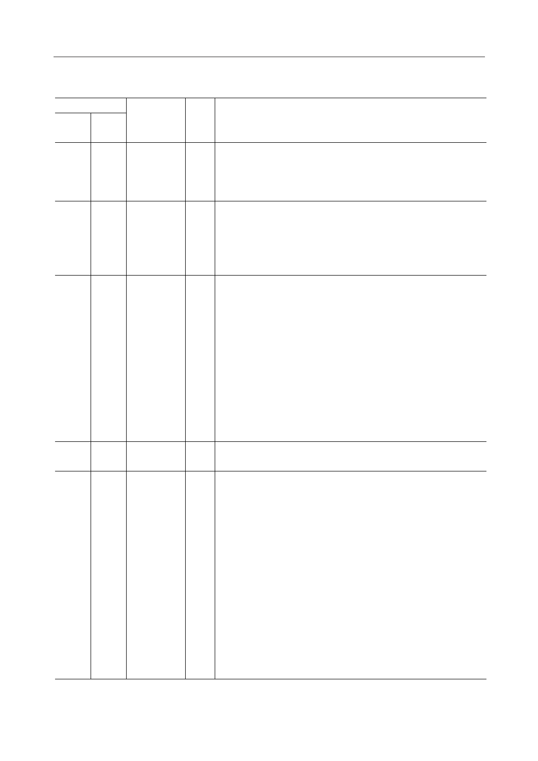
Pin
32-pin 64-pin
SSOP QFP
24
40
25
41
27
44
28
45
29
46
Symbol
SYNCO
SCKO
RST
WDT
GC
Type
Description
O 8 kHz sync signal for the PCM CODEC.
Connect this pin to the SYNC pin and the PCM CODEC transmit/receive
sync pin.
Leave it open if using an external SYNC.
O Transmit clock signal (200 kHz) for the PCM CODEC.
Connect this pin to the SCK pin and the PCM CODEC transmit/receive
clock pin.
Not affected by reset. Outputs "0" during power-down.
Leave it open if using an external SCK.
I Reset signal.
"L": Reset mode
"H": Normal operation mode
During initialization, input signals, except for PWDWN are disabled for
100 ms after reset (after RST is returned from "L" to "H").
Input the basic clock during the reset.
Output pins during reset are in the following sates :
High impedance: SOUT, ROUT, PD0 to 15
"L": WDT
"H": OF1, OF2
Not affected: X2, SYNCO, SCKO, IRLD, MCKO
O Test pin.
Leave this pin open.
I Input signal for the gain controller when RIN input is controlled and the
RIN input level is controlled and howling is prevented.
The gain controller adjusts the RIN input level when it is –20 dBm0 or
above. RIN input levels from –20 to –11.5 dBm0 will be suppressed to
–20 dBm0 in the attenuation range from 0 to 8.5 dB.
RIN input levels above –11.5 dBm0 will always be attenuated by 8.5 dB.
• Single Chip or Master Chip in a Cascade Connection
"H": Gain control ON
"L": Gain control OFF
"H" is recommended for echo cancellation.
• Slave Chip in a Cascade Connection
Fixed at "L"
This pin is loaded in synchronization with the falling edge of the INT
signal or the rising edge of RST.
8/28
Share Link: 