NLAS1053USG(2015) 查看數據表(PDF) - ON Semiconductor
零件编号
产品描述 (功能)
比赛名单
NLAS1053USG Datasheet PDF : 10 Pages
| |||
NLAS1053
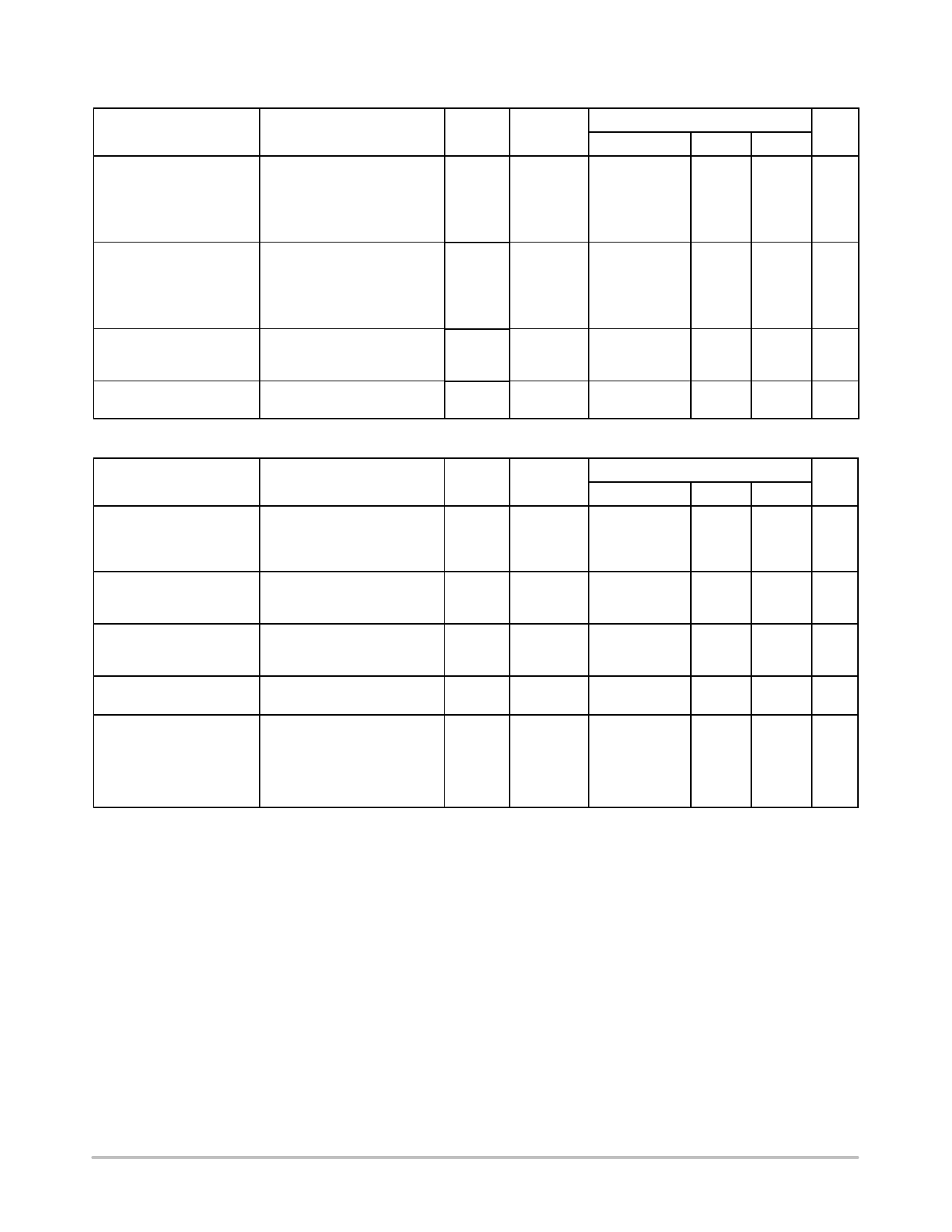
DC CHARACTERISTICS − Digital Section (Voltages Referenced to GND)
Parameter
Minimum High−Level Input
Voltage, Select and Inhibit
Inputs
Condition
Symbol
VCC
VIH
2.0
2.5
3.0
4.5
5.5
Guaranteed Limit
*55_C to 25_C t85_C t125_C Unit
1.5
1.5
1.5
V
1.9
1.9
1.9
2.1
2.1
2.1
3.15
3.15
3.15
3.85
3.85
3.85
Maximum Low−Level Input
Voltage, Select and Inhibit
Inputs
VIL
2.0
2.5
3.0
4.5
5.5
0.5
0.5
0.5
V
0.6
0.6
0.6
0.9
0.9
0.9
1.35
1.35
1.35
1.65
1.65
1.65
Maximum Input Leakage
Current, Select and Inhibit
Inputs
VIN = 5.5 V or GND
IIN
0 V to 5.5 V
$0.1
$1.0 $1.0 mA
Maximum Quiescent Supply Select and Inhibit = VCC or GND ICC
5.5
Current
1.0
1.0
2.0
mA
DC ELECTRICAL CHARACTERISTICS − Analog Section
Parameter
Maximum “ON”
Resistance
(Figures 17 − 23)
Condition
VIN = VIL or VIH
VIS = GND to VCC
IINI ≤ 10.0 mA
Symbol
VCC
RON
2.5
3.0
4.5
5.5
ON Resistance Flatness
(Figures 17 − 23)
VIN = VIL or VIH
IINI ≤ 10.0 mA
VIS = 1V, 2V, 3.5V
RFLAT
4.5
(ON)
ON Resistance Match
Between Channels
VIN = VIL or VIH
IINI ≤ 10.0 mA
VCH1 or VCH0 = 3.5 V
DRON
4.5
(ON)
CH1 or CH0 Off Leakage VIN = VIL or VIH
ICH0
5.5
Current (Figure 9)
VCH1 or VCH0 = 1.0 VCOM 4.5 V
ICH1
COM ON Leakage
Current (Figure 9)
VIN = VIL or VIH
ICOM(ON)
5.5
VCH1 1.0 V or 4.5 V with VCH0
floating or
VCH1 1.0 V or 4.5 V with VCH1
floating
VCOM = 1.0 V or 4.5 V
Guaranteed Limit
-55 to 255C
70
40
20
16
< 855C < 1255C Unit
85
105
W
46
52
28
34
22
28
4
4
5
W
2
2
3
W
1
10
100
nA
1
10
100
nA
www.onsemi.com
3
Share Link: 