GLT6200L16L-55FG 查看數據表(PDF) - G-Link Technology
零件编号
产品描述 (功能)
比赛名单
GLT6200L16L-55FG Datasheet PDF : 13 Pages
| |||
G-LINK
GLT6200L16
Ultra Low Power 128k x 16 CMOS SRAM
May 2001(Rev. 2.3)
Features :
Description :
∗ Low-power consumption.
-active: 30mA Icc at 55ns.
The GLT6200L16 is a low power CMOS Static
RAM organized as 131,072 words by 16 bits. Easy
-stand by :
memory expansion is provided by an active LOW
10 µA (CMOS input / output , LL)
CE1 and OE pin.
2 µA (CMOS input / output, SL)
∗ Single +2.7V to 3.6V power supply.
∗ Equal access and cycle time.
∗ 55\70\85 ns access time.
∗ Tri-state output.
This device has an automatic power – down
mode feature when deselected. Separate Byte
Enable controls ( BLE and BHE ) allow individual
bytes to be accessed. BLE controls the lower bits
∗ Automatic power-down when
I/O0 – I/O7. BHE controls the upper bits I/O8 –
deselected.
I/O15.
∗ Multiple center power and ground pins
Writing to these devices is performed by taking
for improved noise immunity.
Chip Enable CE1 with Write Enable WE and byte
∗ Individual byte controls for both read
and write cycles.
Enable ( BLE / BHE ) Low
∗ Industrial grade (-40°C ~ 85°C)
Reading from the device is performed by taking
available.
Chip Enable CE1 with Output enable OE and byte
∗ Available in 48-fpBGA/44L TSOPII.
Enable ( BLE / BHE ) Low while Write Enable WE
and CE2 are held HIGH.
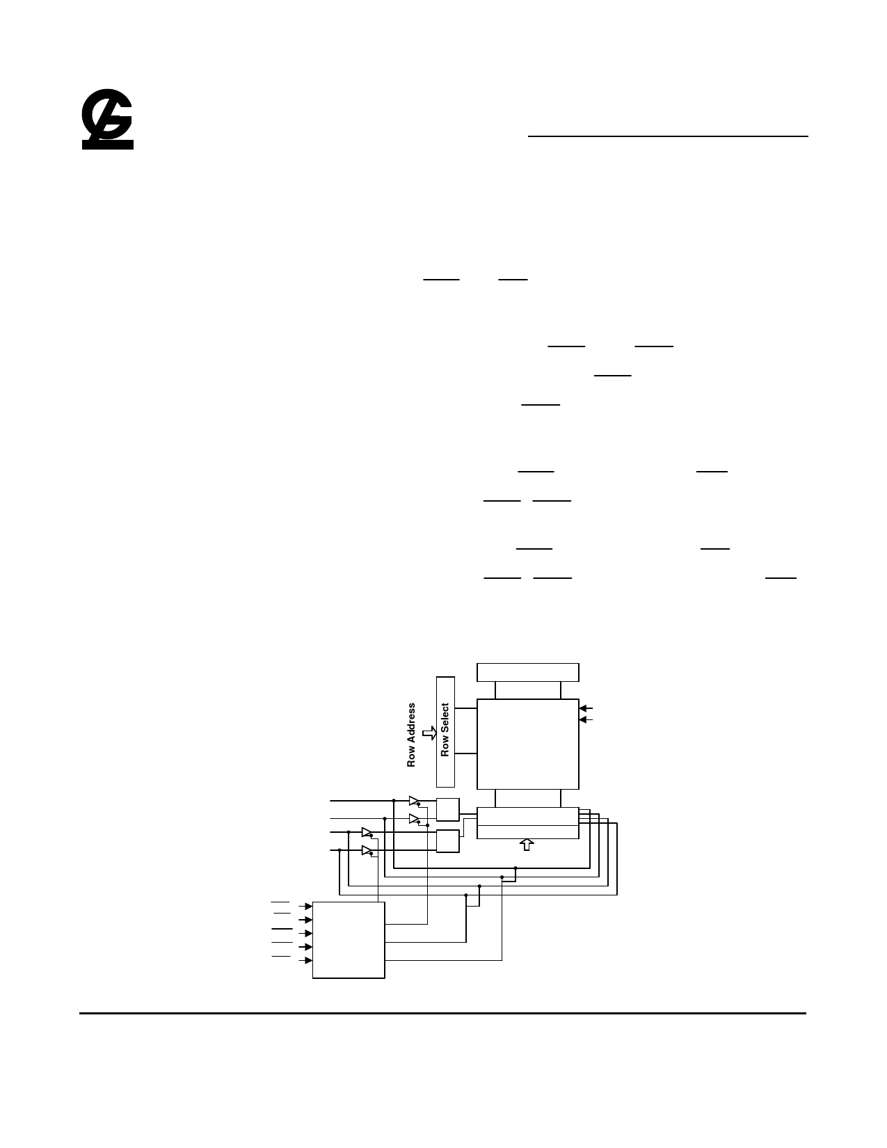
Function Block Diagram :
Pre-Charge Circuit
Vcc
Vss
Memory Array
1024 x 2048
I/O0 - I/O7
I/O8 - I/O15
Data
Circuit
Data
Circuit
I/O Circuit
Column Select
Column Address
WE
OE
BHE
BLE
CE1
Control
Logic
G-Link Technology Corporation
2701 Northwestern Parkway
Santa Clara, CA 95051, U.S.A.
-1-
G-Link Technology Corporation, Taiwan
6F No. 24-2, Industry E. RD. IV, Science Based
Industrial Park, Hsin Chu, Taiwan.
Share Link: 