P4C189 查看數據表(PDF) - Semiconductor Corporation
零件编号
产品描述 (功能)
比赛名单
P4C189 Datasheet PDF : 8 Pages
| |||
P4C189
FUNCTIONAL DESCRIPTION
An active LOW write enable (WE) controls the writing/
reading operation of the memory. When chip select (CS)
and write enable (WE) are LOW, the information on data
inputs (D0 through D3) is written into the addressed memory
word. Reading is performed with chip select (CS) LOW and
write enable (WE) HIGH. The information stored in the
addressed word is read out on the inverting outputs (O
0
through O ). The outputs of the memory go to an inactive
3
high impedance state whenever chip select (CS) is HIGH,
or during the write operation when write enable (WE) is
LOW.
TRUTH TABLE
Mode
CS
WE
Standby
H
X
Read
L
H
Write
L
L
Output
High Z
DOUT
High Z
Notes: H = HIGH
L = Low
X = Don't Care
HIGH Z = Implies outputs are disabled or off. This condition
is defined as high impedance state.
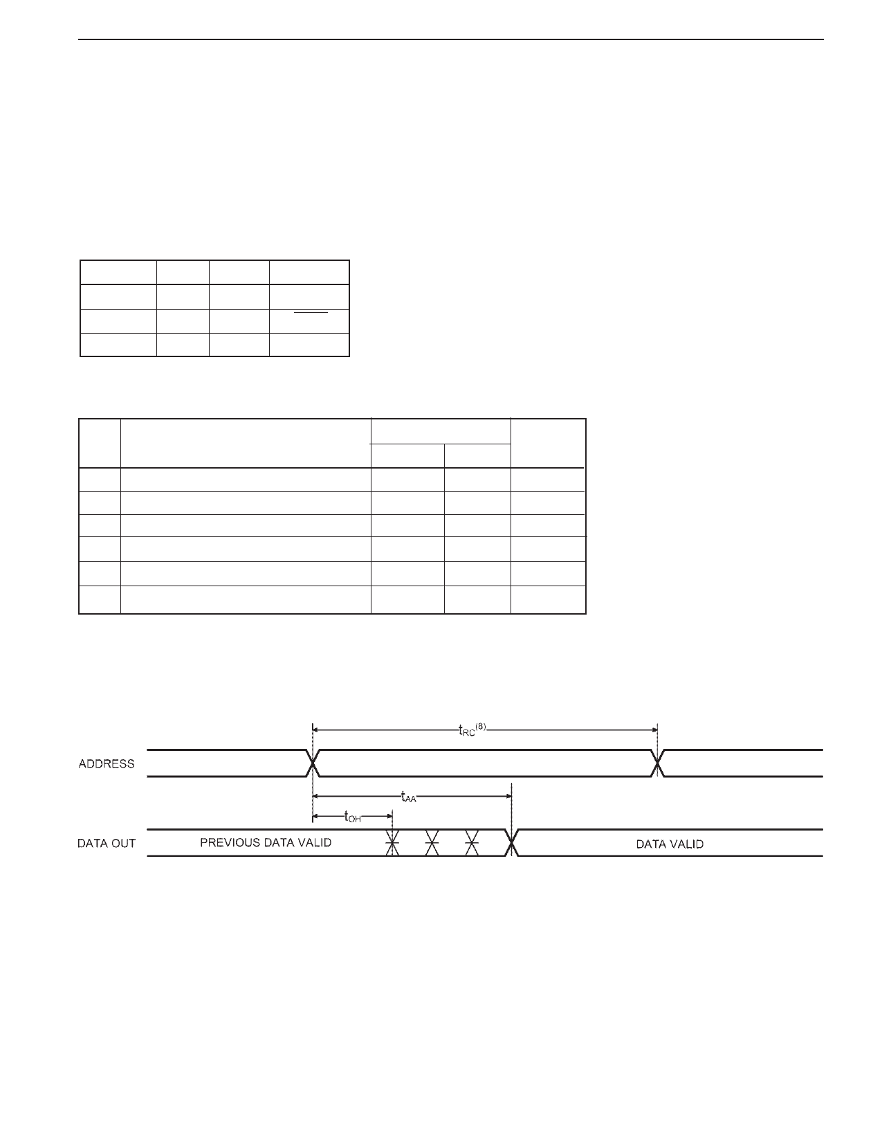
AC CHARACTERISTICS—READ CYCLE
(VCC = 5V ± 10%, All Temperature Ranges)(2)
Sym.
Parameter
-35
Unit
Min
Max
tRC Read Cycle Time
35
tAA Address Access Time
tAC Chip Enable Access Time
tOH Output Hold from Address Change
2
tLZ Chip Enable to Output in Low Z
2
ns
35
ns
15
ns
ns
ns
tHZ Chip Disable to Output in High Z
10
ns
TIMING WAVEFORM OF READ CYCLE NO. 1(5)
Document # SRAM100 Rev OR
Page 3 of 8
Share Link: 