CS5257A-1GDP5 查看數據表(PDF) - Cherry semiconductor
零件编号
产品描述 (功能)
比赛名单
CS5257A-1GDP5 Datasheet PDF : 9 Pages
| |||
Application Notes: continued
While not required, a bypass capacitor connected between
the adjust pin and ground will improve transient response
and ripple rejection. A 0.1µF tantalum capacitor is recom-
mended for Òfirst cutÓ design. Value and type may be var-
ied to optimize performance vs. price.
Other Adjustable Operation Considerations
The CS5257A-1 linear regulator has an absolute maximum
specification of 6V for the voltage difference between VIN
and VOUT. However, the IC may be used to regulate volt-
ages in excess of 6V. The two main considerations in such a
design are the sequencing of power supplies and short cir-
cuit capability.
Power supply sequencing should be such that the VCON-
TROL supply is brought up coincidentally with or before the
VPOWER supply. This allows the IC to begin charging the
output capacitor as soon as the VPOWER to VOUT differential
is large enough that the pass transistor conducts. As VPOW-
ER increases, the pass transistor will remain in dropout, and
current is passed to the load until VOUT is in regulation.
Further increase in the supply voltage brings the pass tran-
sistor out of dropout. In this manner, any output voltage
less than 13V may be regulated, provided the VPOWER to
VOUT differential is less than 6V. In the case where VCON-
TROL and VPOWER are shorted, there is no theoretical limit
to the regulated voltage as long as the VPOWER to VOUT dif-
ferential of 6V is not exceeded.
There is a possibility of damaging the IC when VPOWER-VIN
is greater than 6V if a short circuit occurs. Short circuit con-
ditions will result in the immediate operation of the pass
transistor outside of its safe operating area. Over-voltage
stresses will then cause destruction of the pass transistor
before overcurrent or thermal shutdown circuitry can
become active. Additional circuitry may be required to
clamp the VPOWER to VOUT differential to less than 6V if fail
safe operation is required. One possible clamp circuit is
illustrated in Figure 2; however, the design of clamp cir-
cuitry must be done on an application by application basis.
Care must be taken to ensure the clamp actually protects
the design. Components used in the clamp design must be
able to withstand the short circuit condition indefinitely
while protecting the IC.
External Supply
The capacitor value and type is based on cost, availability,
size and temperature constraints. A tantalum or aluminum
electrolytic capacitor is best, since a film or ceramic capaci-
tor with almost zero ESR can cause instability. The alu-
minum electrolytic capacitor is the least expensive solution.
However, when the circuit operates at low temperatures,
both the value and ESR of the capacitor will vary consider-
ably. The capacitor manufacturer's data sheet provides this
information.
A 300µF tantalum capacitor will work for most applica-
tions, but with high current regulators such as the
CS5257A-1 the transient response and stability improve
with higher values of capacitor. The majority of applica-
tions for this regulator involve large changes in load cur-
rent so the output capacitor must supply the instantaneous
load current. The ESR of the output capacitor causes an
immediate drop in output voltage given by:
ÆV = ÆI ´ ESR.
For microprocessor applications it is customary to use an
output capacitor network consisting of several tantalum
and ceramic capacitors in parallel. This reduces the overall
ESR and reduces the instantaneous output voltage drop
under transient load conditions. The output capacitor net-
work should be as close to the load as possible for the best
results.
Protection Diodes
When large external capacitors are used with a linear
regulator it is sometimes necessary to add protection
diodes. If the input voltage of the regulator gets shorted,
the output capacitor will discharge into the output of the
regulator. The discharge current depends on the value of
the capacitor, the output voltage, and the rate at which
VCONTROL drops. In the CS5257A-1 regulator, the discharge
path is through a large junction and protection diodes are
not usually needed. If the regulator is used with large val-
ues of output capacitance and the input voltage is instanta-
neously shorted to ground, damage can occur. In this case,
a diode connected as shown in Figure 3 is recommended.
Use of the diode has the added benefit of bleeding VOUT to
ground if VCONTROL is shorted. This prevents an unregulat-
ed output from causing system damage.
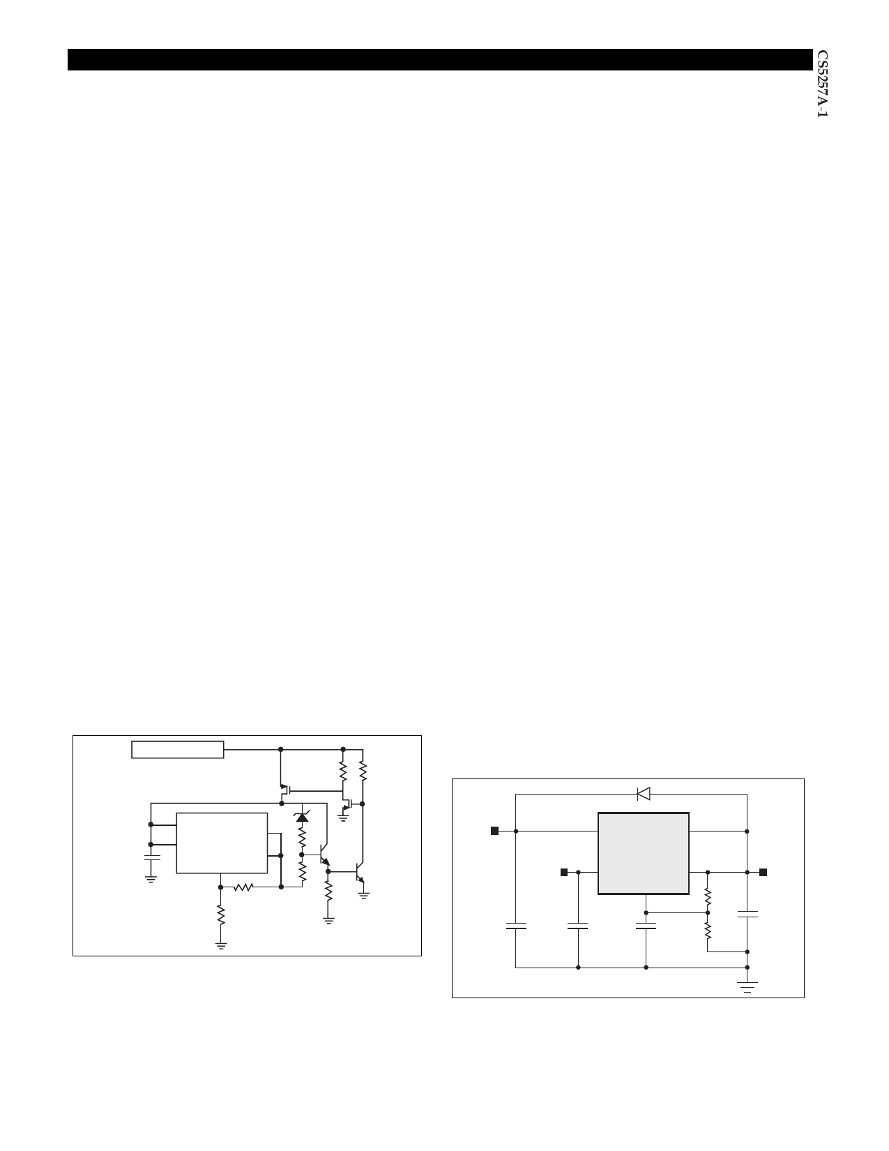
VControl
VSENSE
VPower
VAdjust
VOUT
VCONTROL VOUT
CS5257A-1
VPOWER VSENSE
Adjust
Figure 2: Example clamp circuitry for VPOWER - VOUT > 6V.
Stability Considerations
The output compensation capacitor helps determine three
main characteristics of a linear regulator: start-up delay,
load transient response, and loop stability.
Figure 3: Diode protection against VCONTROL short circuit conditions.
7
Share Link: 