P80C557E4 查看數據表(PDF) - Philips Electronics
零件编号
产品描述 (功能)
比赛名单
P80C557E4 Datasheet PDF : 72 Pages
| |||
Philips Semiconductors
Single-chip 8-bit microcontroller
Product specification
P83C557E4/P80C557E4/P89C557E4
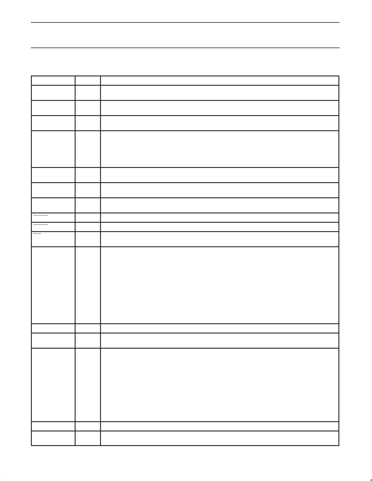
4.1 PIN DESCRIPTION
SYMBOL
AVref–
AVref+
AVSS1
AVDD1
AVSS2
AVDD2
P5.7 – P5.0
PIN
1
2
3
4
77
76
5 – 12
DESCRIPTION
Low end of analog to digital conversion reference resistor
High end of analog to digital conversion reference resistor.
Analog ground for ADC
Analog power supply (+5 V) for ADC
Analog ground; for PLL oscillator
Analog power supply; (+5 V) for PLL oscillator
Port 5
8-bit input port
Port pin
Alternative function
VDD1, VDD2,
VDD3, VDD4
VSS1, VSS2
VSS3, VSS4
ADEXS
PWM0
PWM1
EW
P4.0 – P4.7
RSTIN
RSTOUT
P1.0 – P1.7
14, 28,
53, 66
13, 29,
54, 67
15
16
17
18
19 – 22
24 – 27
30
23
31 – 38
P5.0–P5.7
Eight input channels to ADC (ADC0–ADC7)
Digital power supply: +5 V power supply pins during normal operation and power reduction modes. All pins
must be connected.
Digital ground: circuit ground potential. All pins must be connected.
Start ADC operation: Input starting analog to digital conversion triggered by a programmable edge (ADC
operation can also be started by software). This pin must not float
Pulse width modulation output 0
Pulse width modulation output 1
Enable watchdog timer: Enable for T3 watchdog timer and disable Power-down Mode.This pin must not
float.
Port 4
8-bit quasi-bidirectional I/O port
Port pin
Alternative function
P4.0
P4.1
P4.2
P4.3
P4.4
P4.5
P4.6
P4.7
CMSR0 }
CMSR1 }
CMSR2 } compare and set/reset
CMSR3 } outputs on a match with timer T2
CMSR4 }
CMSR5 }
CMT0 } compare and toggle outputs
CMT1 }
on a match with timer T2
Reset: Input to reset the P8xC557E4.
Reset: Output of the P8xC557E4 for resetting peripheral devices during initialization and Watchdog Timer
overflow.
Port 1
8-bit quasi-bidirectional I/O port
Port pin
Alternative function
SCL
SDA
P1.0
P1.1
P1.2
P1.3
P1.4
P1.5
P1.6
P1.7
CT0I/INT2}
CT1I/INT3} :
CT2I/INT4}
CT3I/INT5}
T2
:
RT2
:
Capture timer inputs for
timer T2 or external interrupt inputs
T2 event input, rising edge triggered
T2 timer reset input, rising edge triggered
39
I2C-bus serial clock I/O port
40
I2C-bus serial data I/O port
If SCL and SDA are not used, they must be connected to VSS.
1999 Mar 02
6
Share Link: 