PCF8584 查看數據表(PDF) - Philips Electronics
零件编号
产品描述 (功能)
比赛名单
PCF8584 Datasheet PDF : 40 Pages
| |||
Philips Semiconductors
I2C-bus controller
Product specification
PCF8584
andbook, full pagewidth
to/from microcontroller parallel bus
DB7 DB6 DB5 DB4 DB3 DB2 DB1 DB0
to/from
I2C-Bus SDA line
Read Buffer
Data Shift Register S0 and Read Buffer
Shift register
Read
only
Write
only
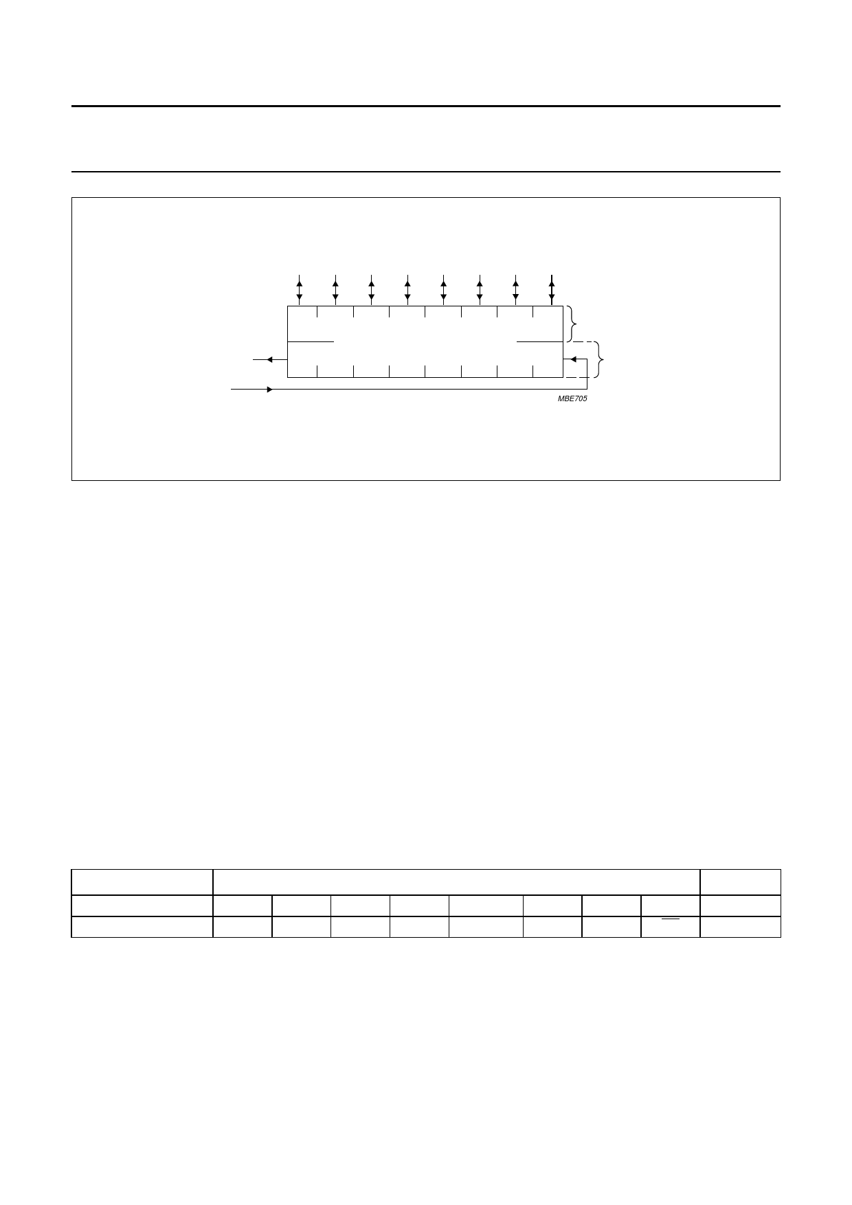
MBE705
Fig.4 Data shift register/bus buffer S0.
In receiver mode the data from the shift register is copied to the read buffer during the acknowledge phase. Further
reception of data is inhibited (SCL held LOW) until the S0 read buffer is read (see Section 6.8.1.1).
In the transmitter mode data is transmitted to the I2C-bus as soon as it is written to the S0 shift register if the serial I/O is
enabled (ESO = 1).
Remarks:
1. A minimum of 6 clock cycles must elapse between consecutive parallel-bus accesses to the PCF8584 when the
I2C-bus controller operates at 8 or 12 MHz. This may be reduced to 3 clock cycles for lower operating frequencies.
2. To start a read operation immediately after a write, it is necessary to read the S0 read buffer in order to invoke
reception of the first byte (‘dummy read’ of the address). Immediately after the acknowledgement, this first byte will
be transferred from the shift register to the read buffer. The next read will then transfer the correct value of the first
byte to the microcontroller bus (see Fig.7).
6.8 Control/status register S1
Register S1 controls I2C-bus operation and provides I2C-bus status information. Register S1 is accessed by a HIGH
signal on register select input A0. For more efficient communication between microcontroller/processor and the I2C-bus,
register S1 has separate read and write functions for all bit positions (see Fig.3). The write-only section provides register
access control and control over I2C-bus signals, while the read-only section provides I2C-bus status information.
Table 4 Control/status register S1
CONTROL/STATUS
Control(1)
PIN
Status(2)
PIN
ESO
0(3)
ES1
STS
Notes
1. For further information see Section 6.8.1.
2. For further information see Section 6.8.2.
3. Logic 1 if not-initialized.
BITS
ES2
ENI
BER AD0/LRB
STA
AAS
STO
LAB
ACK
BB
MODE
write only
read only
1997 Oct 21
9
Share Link: 