PCK2002DGG 查看數據表(PDF) - Philips Electronics
零件编号
产品描述 (功能)
比赛名单
PCK2002DGG Datasheet PDF : 12 Pages
| |||
Philips Semiconductors
0–300 MHz I2C 1:18 clock buffer
Product data
PCK2002
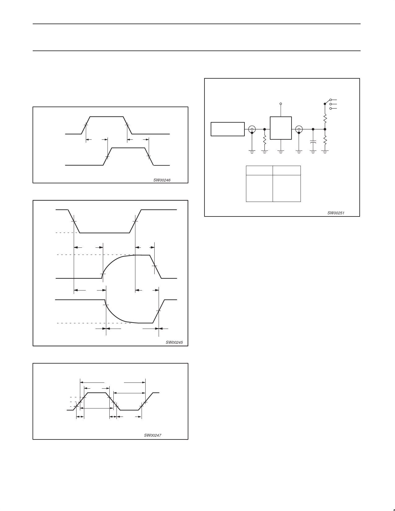
AC WAVEFORMS
VM = 1.5 V
VX = VOL + 0.3 V
VY = VOH –0.3 V
VOL and VOH are the typical output voltage drop that occur with the
output load.
BUF_IN
INPUT
VM
tPLH
VDD
VM
tPHL
BUF_OUT
VM
VM
SW00246
Figure 1. Load circuitry for switching times.
VI
VDD
nOE INPUT
VM
GND
VDD
OUTPUT
LOW-to-OFF
OFF-to-LOW
VOL
tPLZ
VX
tPZL
VM
VOH
OUTPUT
HIGH-to-OFF
OFF-to-HIGH
VSS
tPHZ
outputs
enabled
tPZH
VY
outputs
disabled
VM
outputs
enabled
SW00245
Figure 2. 3-State enable and disable times
TEST CIRCUIT
VDD
PULSE
GENERATOR
VI
RT
D.U.T.
VO
CL
S1
2<VDD
Open
VSS
500Ω
500Ω
TEST
tPLH/tPHL
tPLZ/tPZL
tPHZ/tPZH
S1
Open
2<VDD
VSS
SW00251
Figure 4. Load circuitry for switching times
TSDKH
TSDKP
DUTY CYCLE
2.4
1.5
0.4
TSDRISE
TSDKL
TSDFALL
SW00247
Figure 3. Buffer Output clock
2001 Jul 19
9
Share Link: 