PDI1394L40 查看數據表(PDF) - Philips Electronics
零件编号
产品描述 (功能)
比赛名单
PDI1394L40 Datasheet PDF : 80 Pages
| |||
Philips Semiconductors
1394 enhanced AV link layer controller
Preliminary specification
PDI1394L40
1.0 FEATURES
• IEEE1394a and IEEE1394–1995 Standard Link Layer Controller
• Hardware Support for the IEC61883 International Standard of
Digital Interface for Consumer Electronics
• Interface to any IEEE 1394–1995 or 1394a Physical Layer
Interface
• 5 V Tolerant I/Os
• Single 3.3 V supply voltage
• Full-duplex isochronous operation
• Operates with 400/200/100 Mbps physical layer devices
• 12K byte fully programmable FIFO pool for isochronous and
asynchronous data
• Supports single capacitor isolation mode and IEEE 1394–1995,
Annex J. isolation
• 6-field deep SYT buffer added to enhance real-time isochronous
synchronization using the AVFSYNC pin
• Generates its own AV port clocks under software control. Select
one of three frequencies: 24.576, 12.288, or 6.144 MHz
• On chip timer resources
• Flexible 8/16 bit multiplexed/non-multiplexed host interface
• Parallel AV interface
2.0 DESCRIPTION
The PDI11394L40, Philips Semiconductors Full Duplex 1394
Audio/Video (AV) Link Layer Controller, is an IEEE 1394a–2000
compliant link layer controller featuring 2 embedded AV layer
interfaces.
The application data is packetized according to the IEC 61883
International Standard of Interface for Consumer Electronic
Audio/Video Equipment. Both AV layer interfaces are byte-wide
ports capable of accommodating various MPEG–2 and DVC
codecs. A flexible host interface is provided for internal register
configuration as well as performing asynchronous data transfers.
Both 8 bit and 16 bit wide data paths, as well as
multiplexed/non-multiplexed access modes are supported.
The PDI1394L40 is powered by a single 3.3 V power supply and the
inputs and outputs are 5 V tolerant. It is available in the LQFP144
package.
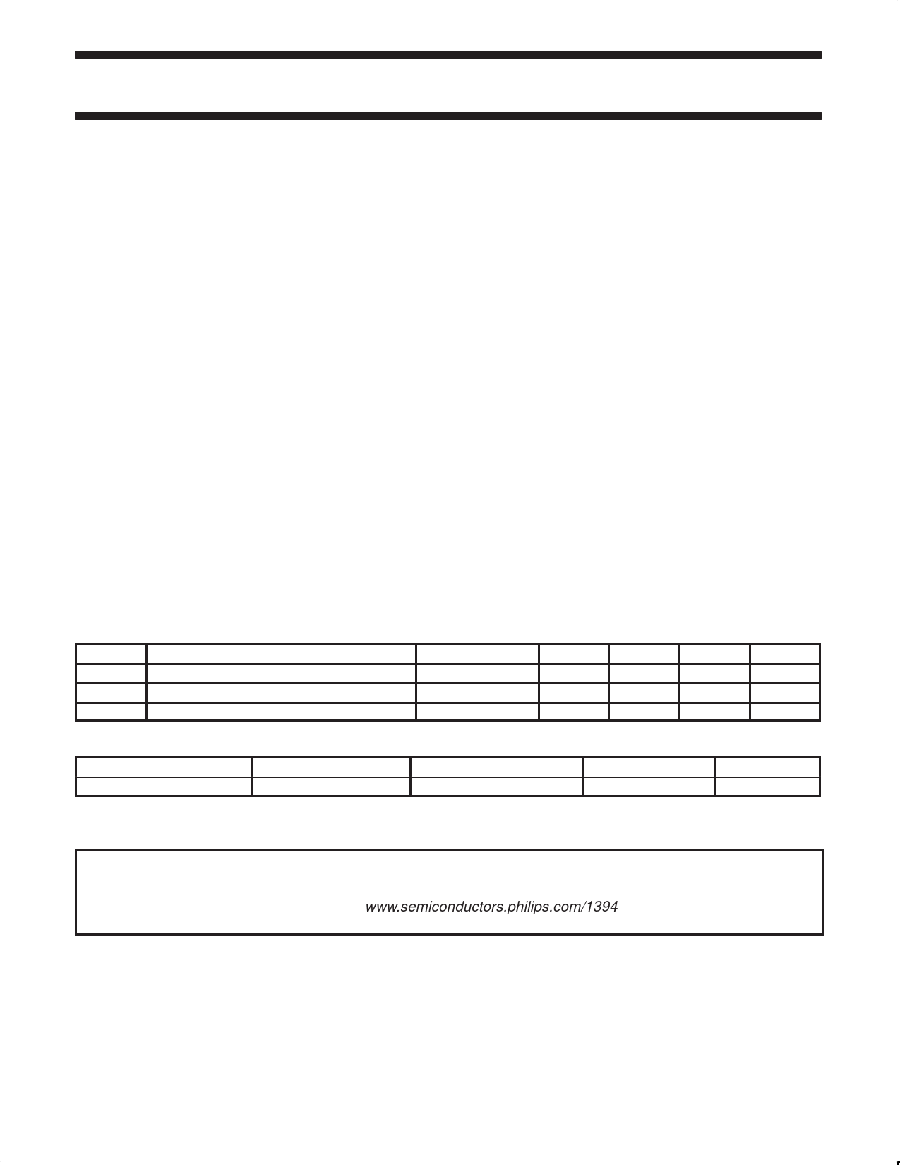
3.0 QUICK REFERENCE DATA
GND = 0 V; Tamb = 25 °C
SYMBOL
PARAMETER
VDD
IDD
SCLK
Functional supply voltage range
Supply current @ VDD = 3.3 V
Device clock
CONDITIONS
Operating
MIN
3.0
49.147
TYP
3.3
110
49.152
MAX
3.6
200
49.157
UNIT
V
mA
MHz
4.0 ORDERING INFORMATION
PACKAGES
TEMPERATURE RANGE
144-pin LQFP144
0 to +70 °C
OUTSIDE NORTH AMERICA
PDI1394L40BE
NORTH AMERICA
PDI1394L40BE
PKG. DWG. #
SOT486–1
NOTE:
This datasheet is subject to change.
Please visit our internet website www.semiconductors.philips.com/1394 for latest changes.
2000 Dec 15
1
Share Link: 