PDI1394P22BD 查看數據表(PDF) - Philips Electronics
零件编号
产品描述 (功能)
比赛名单
PDI1394P22BD Datasheet PDF : 30 Pages
| |||
Philips Semiconductors
3-port physical layer interface
Objective specification
PDI1394P22
13.0 THERMAL CHARACTERISTICS
SYMBOL
PARAMETER
TEST CONDITION
RΘjA Junction-to-free-air thermal resistance Board mounted, no air flow
LIMITS
UNIT
MIN
TYP MAX
TBD
°C/W
14.0 AC CHARACTERISTICS
SYMBOL
PARAMETER
Transmit jitter
Transmit skew
tr
TPA, TPB differential output voltage rise time
tf
TPA, TPB differential output voltage fall time
tSU
Setup time, CTL0, CTL1, D1–D7, LREQ to SYSCLK
tH
Hold time, CTL0, CTL1, D1–D7, LREQ after SYSCLK
tD
Delay time SYSCLK to CTL0, CTL1, D1–D7
CONDITION
TPA, TPB
Between TPA and TPB
10% to 90%; At 1394 connector
90% to 10%; At 1394 connector
50% to 50%; See Figure 2
50% to 50%; See Figure 2
50% to 50%; See Figure 3
MIN TYP MAX UNIT
0.15
ns
0.10
ns
0.5
1.2
ns
0.5
1.2
ns
5
ns
0
ns
0.5
11
ns
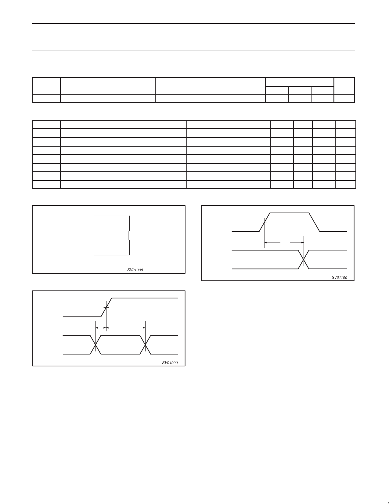
15.0 TIMING WAVEFORMS
TPAn+
TPBn+
56 Ω
TPAn–
TPBn–
SV01098
Figure 1. Test load diagram
SYSCLK
tD
Dn, CTLn, LREQ
SV01100
Figure 3. Dn, CTLn, output delay relative to SYSCLK
SYSCLK
Dn, CTLn, LREQ
tSU
tH
SV01099
Figure 2. Dn, CTLn, LREQ input setup and hold times
1999 Jul 09
11
Share Link: 