PDI1394P23 查看數據表(PDF) - Philips Electronics
零件编号
产品描述 (功能)
比赛名单
PDI1394P23 Datasheet PDF : 42 Pages
| |||
Philips Semiconductors
2-port/1-port 400 Mbps physical layer interface
Preliminary data
PDI1394P23
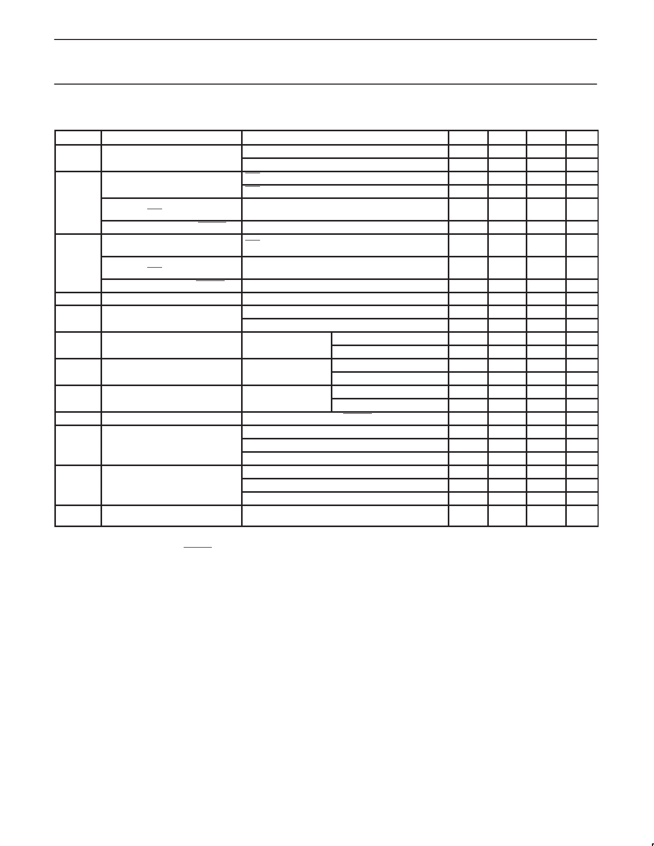
9.0 RECOMMENDED OPERATING CONDITIONS
SYMBOL
PARAMETER
CONDITION
MIN
VDD Supply voltage
Source power node
Non-source power node
3.0
2.7 1
High-level input voltage, LREQ,
ISO = VDD, VDD >= 2.7 V
CTL0, CTL1, D0-D7
ISO = VDD, VDD >= 3.0 V
VIH
High-level input voltage, C/LKON2,
PC0–PC2, ISO, PD
2.3
2.6
0.7 VDD
High-level input voltage, RESET
Low-level input voltage, LREQ,
CTL0, CTL1, D0–D7
ISO = VDD
VIL
Low-level input voltage, C/LKON2,
PC0–PC2, ISO, PD,
0.6 VDD
—
—
Low-level input voltage, RESET
—
IO
Output current
TPBIAS outputs
–6
TPA, TPB cable inputs, during data reception
118
VID
Differential input voltage amplitude
TPA, TPB cable inputs, during data arbitration
168
VIC-100
TPB common-mode input voltage
Speed signaling off Source power node
or S100 speed signal Non-source power node
1.165
1.165
VIC-200 TPB common-mode input voltage S200 speed signal
Source power node
Non-source power node
0.935
0.935
VIC-400 TPB common-mode input voltage S400 speed signal
Source power node
Non-source power node
0.523
0.523
tPU
Power-up reset time
Receive input jitter
Set by capacitor between RESET pin and GND
2
TPA, TPB cable inputs, S100 operation
—
TPA, TPB cable inputs, S200 operation
—
TPA, TPB cable inputs, S400 operation
—
Receive input skew
Between TPA and TPB cable inputs, S100 operation —
Between TPA and TPB cable inputs, S200 operation —
Between TPA and TPB cable inputs, S400 operation —
fXTAL
Crystal or external clock frequency
Crystal connected according to Figure 10 or external
clock input at pin XI
24.5735
NOTES:
1. For a node that does not source power to the bus (see Section 4.2.2.2 in the IEEE 1394-1995 standard).
2. C/LKON is only an input when RESET = 0.
TYP
3.3
3.0
—
—
—
—
—
—
—
—
—
—
—
—
—
—
—
—
—
—
—
—
—
—
24.576
MAX
3.6
3.6
—
—
—
—
0.7
0.2 VDD
0.3 VDD
2.5
260
265
2.515
2.0151
2.515
2.0151
2.515
2.0151
—
1.08
0.5
0.315
0.8
0.55
0.5
24.5785
UNIT
V
V
V
V
V
—
V
V
—
mA
mV
mV
V
V
V
V
V
V
ms
ns
ns
ns
ns
ns
ns
MHz
2001 Sep 06
11
Share Link: 