3340-00 查看數據表(PDF) - Peregrine Semiconductor Corp.
零件编号
产品描述 (功能)
比赛名单
3340-00 Datasheet PDF : 12 Pages
| |||
PE3340
Advance Information
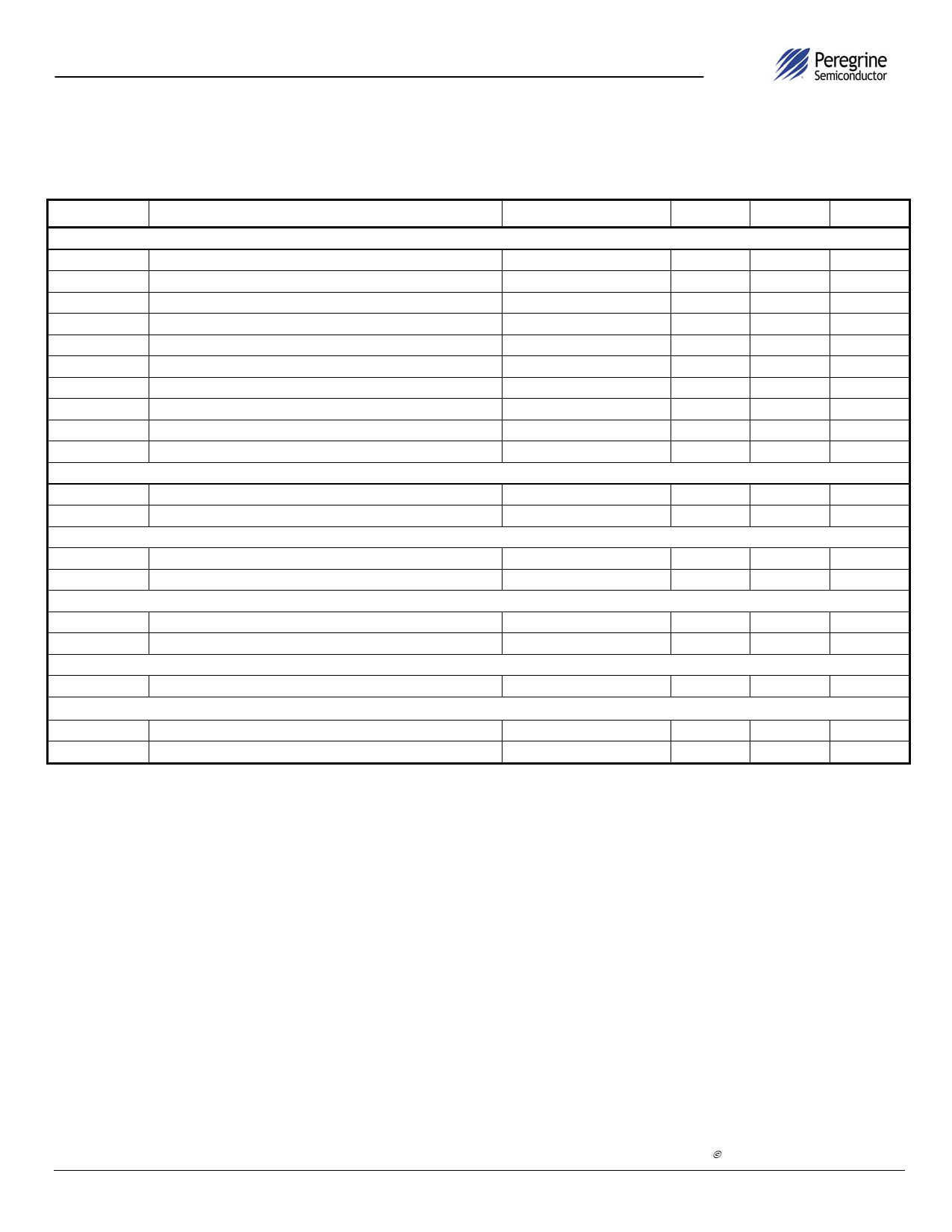
Table 6. AC Characteristics
VDD = 3.0 V, -40° C < TA < 85° C, unless otherwise specified
Symbol
Parameter
Conditions
Control Interface and Latches (see Figures 3, 4)
fClk
Serial data clock frequency
(Note 1)
tClkH
Serial clock HIGH time
tClkL
Serial clock LOW time
tDSU
Sdata set-up time to Sclk rising edge
tDHLD
Sdata hold time after Sclk rising edge
tPW
S_WR pulse width
tCWR
Sclk rising edge to S_WR rising edge
tCE
Sclk falling edge to E_WR transition
tWRC
S_WR falling edge to Sclk rising edge
tEC
E_WR transition to Sclk rising edge
Main Divider (Including Prescaler)
Fin
Operating frequency
PFin
Input level range
External AC coupling
Main Divider (Prescaler Bypassed)
Fin
Operating frequency
PFin
Input level range
External AC coupling
Reference Divider
fr
Operating frequency
(Note 3)
Pfr
Reference input power (Note 2)
Single ended input
Phase Detector
fc
Comparison frequency
(Note 3)
SSB Phase Noise (Fin = 1.3 GHz, fr = 10 MHz, fc = 1.25 MHz, LBW = 70 kHz, VDD = 3.0 V, Temp = -40° C)
100 Hz Offset
1 kHz Offset
Min
Max
Units
10
MHz
30
ns
30
ns
10
ns
10
ns
30
ns
30
ns
30
ns
30
ns
30
ns
500
3000
MHz
-5
5
dBm
50
300
MHz
-5
5
dBm
100
MHz
-2
dBm
20
MHz
-75
dBc/Hz
-85
dBc/Hz
Note 1: fclk is verified during the functional pattern test. Serial programming sections of the functional pattern are clocked at 10 MHz to verify fclk
specification.
Note 2: CMOS logic levels can be used to drive reference input if DC coupled. Voltage input needs to be a minimum of 0.5 Vp-p. For optimum phase
noise performance, the reference input falling edge rate should be faster than 80mV/ns.
Note 3: Parameter is guaranteed through characterization only and is not tested.
PEREGRINE SEMICONDUCTOR CORP. ® | http://www.psemi.com
Copyright © Peregrine Semiconductor Corp. 2004
Page 5 of 12
Share Link: 