4250 查看數據表(PDF) - Peregrine Semiconductor Corp.
零件编号
产品描述 (功能)
比赛名单
4250 Datasheet PDF : 9 Pages
| |||
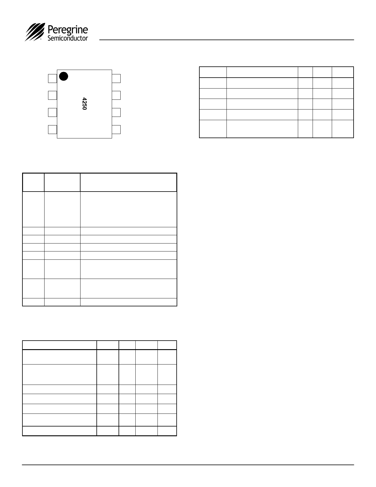
Figure 3. Pin Configuration (Top View)
V2 1
V1 2
8 RF2
7 GND
RFC 3
6 GND
N/C or 4
GND
5 RF1
Table 2. Pin Descriptions
Pin
No.
Pin Name
Description
This pin supports two interface options:
Single-pin control mode. A nominal 3-volt
1
V2
or 5-volt supply connection is required.
Complementary-pin control mode. A
complementary CMOS control signal
to V1 is supplied to this pin.
2
V1
Switch control input, CMOS logic level.
3
RFC
RF Common port.3
4
N/C or GND No Connect or Ground
5
RF13
RF1 port.3
Ground Connection. Traces should be
6
GND
physically short and connected to ground
plane for best performance.
Ground Connection. Traces should be
7
GND
physically short and connected to ground
plane for best performance.
8
RF23
RF2 port.3
Note 3. All RF pins must be DC blocked with an external
series capacitor or held at 0 VDC.
Table 3. Operating Ranges
Parameter
Min Typ Max Units
VDD Power Supply Voltage4
3.0 3.3 3.6
V
4.5 5.0 5.5
V
IDD Power Supply Current
VDD = VCNTL= 3.3V
VDD = VCNTL= 5.0V
55
60
µA
75
80
µA
Control Voltage High
0.8 x VDD
V
Control Voltage Low
0.2 x VDD V
PIN RF Input Power (50Ω)
27
TOP Operating temperature
range
-40
25
85
TST Storage temperature range
-65
25
150
Note 4. Customer must choose either 3.3 V or 5.0 V power
supply range
dBm
°C
°C
©2008-2009 Peregrine Semiconductor Corp. All rights reserved.
Page 2 of 9
PE4250
Product Specification
Table 4. Absolute Maximum Ratings
Symbol Parameter/Conditions Min Max Units
VDD
VI
TST
PIN
VESD
Power supply voltage
3 5.5
Voltage on any control input -0.3 5.5
Storage temperature range
RF Input power (50Ω)
-65 150
27
ESD voltage (HBM)5
ESD voltage (Machine Model)
4000
250
V
V
°C
dBm
V
Note: 5. Human Body Model (HBM, MIL_STD 883 Method 3015.7)
Exceeding absolute maximum ratings may cause
permanent damage. Operation should be
restricted to the limits in the Operating Ranges
table. Operation between operating range
maximum and absolute maximum for extended
periods may reduce reliability.
Latch-Up Avoidance
Unlike conventional CMOS devices, UltraCMOS™
devices are immune to latch-up.
Electrostatic Discharge (ESD) Precautions
When handling this UltraCMOS™ device, observe
the same precautions that you would use with
other ESD-sensitive devices. Although this device
contains circuitry to protect it from damage due to
ESD, precautions should be taken to avoid
exceeding the specified rating.
Switching Frequency
The PE4250 has a maximum 25 kHz switching rate.
Moisture Sensitivity Level
The Moisture Sensitivity Level rating for the PE4250
in the 8-lead MSOP package is MSL1.
Document No. 70-0254-02 │ UltraCMOS™ RFIC Solutions
Share Link: 