PMB2208 查看數據表(PDF) - Infineon Technologies
零件编号
产品描述 (功能)
比赛名单
PMB2208 Datasheet PDF : 27 Pages
| |||
Confidential
PMB 2208
preliminary
Reference
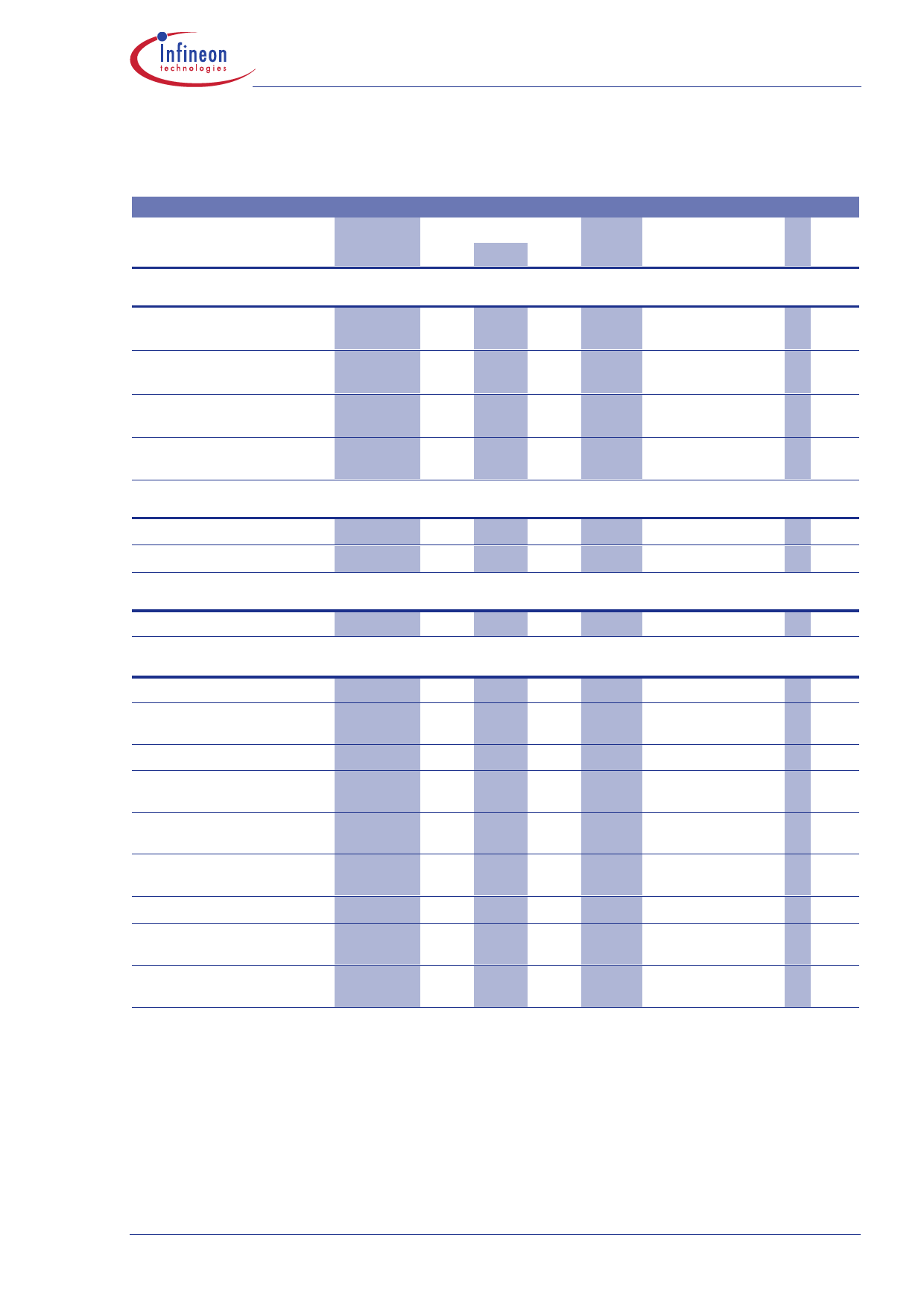
Table 5-3 AC/DC Characteristics with TA =+25 °C, VCC =2.7 to 4.5V (continued)
Symbol
Limit Values
Unit Test Conditions
min typ max
L Item
Modulator inputs A/AX and B/BX: 9A = 9AX = 9B = 9BX = 1.75V
Differential input Resistance 5A-AX
250
5B-BX
Differential input Capacitance &A-AX
1
&B-BX
Input DC current
,A ,AX
,B ,BX
2.5
5.0
10
Differential input
offset current
,OSA ,OSB
-1
1
kΩ I =100kHz
pF I =100kHz
µA Differential input
voltage = 0V
µA
s 13
s 14
15
16
Modulator inputs LO/LOX:
Differential input Resistance
Differential input Capacitance
5LO-LOX
&LO-LOX
4
kΩ I/2 =350MHz
s 17
0.4
pF I/2 =350MHz
s 18
Reference voltage output TREF for A/AX and B/BX inputs:
Output voltage
9TREF
1.65 1.75 1.85
V
19
Modulator output E/EX: 3LO = -10dBm, IA-AX = IB-BX = 455kHz, 9A-AX = 9B-BX = 1Vpp, 90° phase shift
Output power
3E
-7
-4
-1
dBm
Output power with
3E4)
power matching
0
dBm Application circuit
Carrier suppression
DC6)
33
48
dB
Single sideband
supression
DSSB
35
49
dB
Suppression of third order
D 7)
IM3
45
51
dB
intermodulation products
Output noise floor
3N5)
-144
dBc/ 20MHz from carrier
Hz Application circuit
Differential output resistance 5E-EX
20
kΩ I( =175MHz
Differential output capaci-
tance
&E-EX
0.4
pF I( =175MHz
RMS phase error of output
φe
signal
0.4
1.0
Degree
s This value is only measured in lab.
* guaranteed by design
20
s 21
22
23
24
s 25
s 26
s 27
28
Wireless Components
5-5
Specification, August 1999
Share Link: 