SA2002 查看數據表(PDF) - South African Micro Electronic Systems
零件编号
产品描述 (功能)
比赛名单
SA2002
South African Micro Electronic Systems

SA2002 Datasheet PDF : 12 Pages
| |||
SA2002H
sames
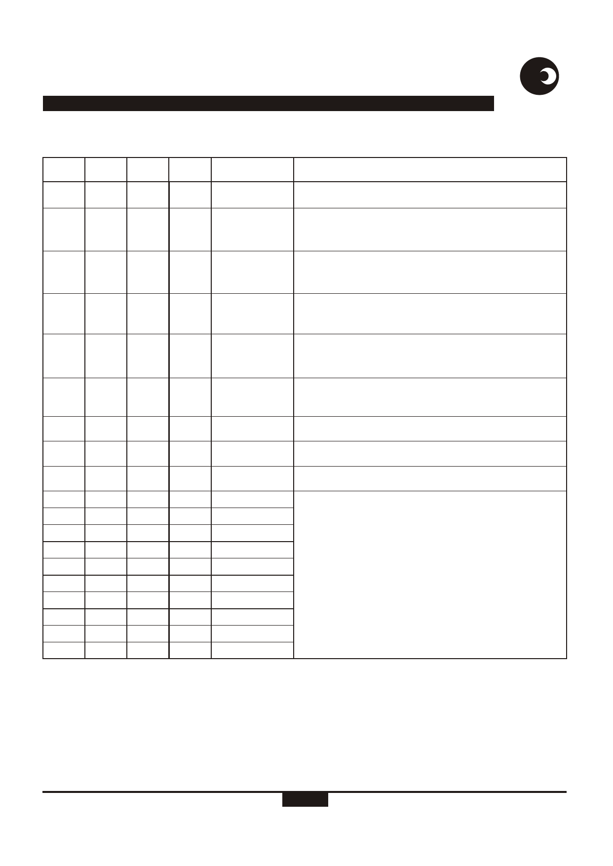
PIN DESCRIPTION
8
14
16
20
Pin
Pin
Pin
Pin
8
14
16
20
4
5
5
8
6
10
9
14
7
13
15
19
1, 2
1, 2
1, 2
1, 2
3
3
3
3
5
8
6
12
N.A.
9
7
13
N.A.
11
11
15
4
4
4
6
8
5
7
10
6
12
12
7
13
9
14
10
11
16
17
18
Designation
GND
VDD
Description
Analog Ground. The voltage to this pin should be mid-way
between VDD and VSS.
Positive supply voltage. The voltage to this pin is typically +2.5V
if a shunt resistor is used for current sensing or in the case of a
current transformer a +5V supply can be applied.
VSS
IVP
IIN, IIP
VREF
FOUT
DIR
FMO
TP1
TP2
TP3
TP4
TP5
TP6
TP7
TP8
TP9
TP10
Negative supply voltage. The voltage to this pin is typically -2.5V
if a shunt resistor is used for current sensing or in the case of a
current transformer a 0V supply can be applied.
Analog Input for Voltage. The current into the A/D converter
should be set at 14µARMS at nominal mains voltage. The
voltage sense input saturates at an input current of ±25µA peak.
Inputs for current sensor. The shunt resistor voltage from each
channel is converted to a current of 16µARMS at rated conditions.
The current sense input saturates at an input current of ±25µA
peak.
This pin provides the connection for the reference current setting
resistor. A 24kW resistor connected to VSS set the optimum
operating condition.
Pulse rate output. Refer to pulse output format for a description
of the pulse rate.
Direction output. The direction of the energy flow is indicated on
this output.
Voltage sense zero crossover. The FMO output generates pulses
on energy rising edge of the mains voltage.
Leave pins unconnected.
http://www.sames.co.za
3/12
Share Link: