SAF-XC835MT-2FGI 查看數據表(PDF) - Infineon Technologies
零件编号
产品描述 (功能)
比赛名单
SAF-XC835MT-2FGI Datasheet PDF : 56 Pages
| |||
XC835/836
General Device Information
2
General Device Information
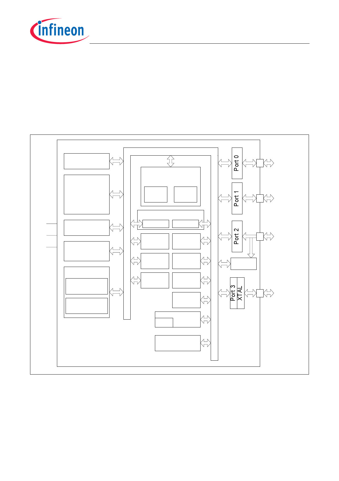
Chapter 2 contains the block diagram, pin configurations, definitions and functions of the
XC835/836.
2.1
Block Diagram
The block diagram of the XC835/836 is shown in Figure 2.
XC83x
8-Kbyte
Boot ROM1)
256-byte RAM
+
64-byte monitor
RAM
VDDP
VSSP
256-byte XRAM
VSSC
4/8-Kbyte
Flash
Clock Generator
48 MHz
On-chip OSC
75 KHz
On-chip OSC
Internal Bus
XC800 Core
T0 & T1 UART
Vector Computer
CORDIC
MDU
RTC
IIC
WDT
SSC
Timer 2 CCU6
OCDS
EVR SCU
1) Includes 1-Kbyte monitor ROM
LED and Touch
Sense Controller
P0.0 - P0.7
P1.0 - P1.5
P2.0 – P2.7
ADC
P3.0 - P3.2
Figure 2 XC835/836 Block Diagram
Data Sheet
5
V1.2, 2011-03
Share Link: 