SC1176 查看數據表(PDF) - Semtech Corporation
零件编号
产品描述 (功能)
比赛名单
SC1176 Datasheet PDF : 23 Pages
| |||
SC1176/SC1176A
POWER MANAGEMENT
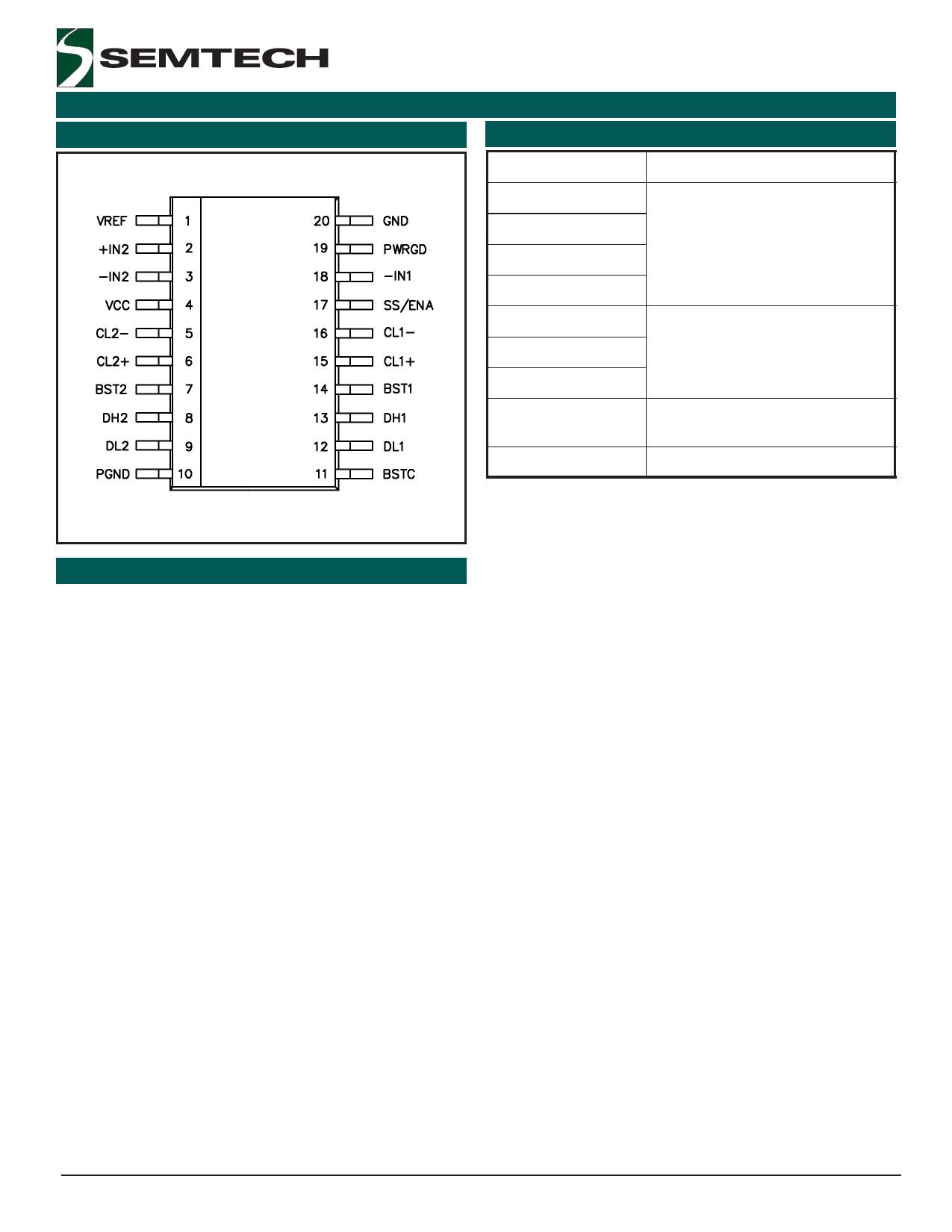
Pin Configuration
Top View
(SOIC-20 and TSSOP-20 Pin)
Ordering Information
Device(1)
Package(2)
SC1176CSWTR
SC1176CSWTRT
SOIC-20
SC1176ASWTR
SC1176ASWTRT
SC1176TSTR
SC1176TSTRT
TSSOP-20
SC1176ATSTR
SC1176EVB-1
Current Share Version Evaluation
Board
SC1176-2EVB-2
Dual Channel Version Evaluation
Notes:
(1) Only available in tape and reel packaging. A reel
contains 1000 (SOIC) or 2500 (TSSOP) devices.
Pin Descriptions
EXPANDED PIN DESCRIPTION
(2) Lead free product. This product is fully WEEE and
RoHS compliant.
Pin 1: (VREF)
Internal .9V reference
Connected to the + input of the master channel error
amplifier.
Pin 2: (+IN2)
+ Input of slave channel error amplifier.
Connected to .9V reference (Pin 1) for
2 independent channel configuration.
Pin 3, 18: (-IN2, -IN1)
- Inputs of close loop error amplifiers.
Works as a feedback inputs (For both modes).
Pin 4: (VCC)
VCC chip supply voltage.
15V maximum, 15mA typical.
Needs a 1µF ceramic multilayer decoupling capacitor
to GND (Pin 20).
Pin 5, 6,15, 16: (CL2-, CL2+, CL1+, CL1-)
Pins (-) and (+) of the current limit amplifiers for both
channels.
Connected to output current sense resistors. Com-
pares that sense voltage to internal 75mV reference.
Needs RC filter for noise rejection.
Pin 7, 14: (BST2, BST1)
BST signal. Supply for high side driver.
Can be connected to a high enough voltage source.
Usually connected to bootstrap circuit.
Pin 8, 13: (DH2, DH1)
DH signal (Drive High).
Gate drive for top MOSFETs.
Requires a small serie resistor.
Pin 9, 12: (DL2, DL1)
DL signal (Drive Low).
Gate drive for bottom MOSFETs.
Requires a small serie resistor.
Pin 10: (PGND)
Power GND. Return of gate drive currents.
Pin 11: (BSTC)
Supply for bottom MOSFETs gate drive.
Pin 17: (SS/ENA)
Soft start pin. Internal current source connected to
external capacitor.
Inhibits he chip if pulled down.
Pin 19: (PWRGD)
Power good signal.
Open collector signal .
Turns to 0 if output voltage is outside the power good
window.
Pin 20: (GND)
Analog GND.
Return of analog signals and bias of chip.
2006 Semtech Corp.
5
www.semtech.com
Share Link: 