SC1633 查看數據表(PDF) - Semtech Corporation
零件编号
产品描述 (功能)
比赛名单
SC1633 Datasheet PDF : 7 Pages
| |||
January 29, 1998
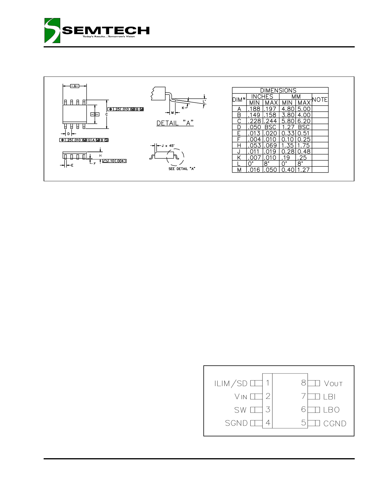
DEVICE OUTLINE - SO-8
LOW VOLTAGE STEP-UP
DC-DC CONVERTER
SC1633
PIN DESCRIPTIONS
PIN 1: ILIM/SD (1) Connected to VIN pin through a
resistor to set the switch peak current.
It serves to protect the IC and induc-
tor, as well as to improve efficiency
and output ripple. However, the supply
capability of the SC1633 is limited by
the current limit resistor (see typical
performance characteristics). The
ILIM/SD pin should be shorted to VIN if
limiting switch peak current is not
required.
(2) The SC1633 goes into shutdown
mode and consumes less than 10µA
when the ILIM/SD pin is pulled to
ground.
PIN 2: VIN
PIN 3: SW
Input supply.
Drain of the power switch, to be con-
nected to the inductor and diode.
PIN 4: SGND Ground connected to the source of the
power switch.
PIN 5: CGND Ground for control circuits of the IC. It
should be separated from SGND to
avoid interference.
PIN 6: LBO
Open drain output of the battery low
detector, with 45 Ohm “On Resis-
tance” at VIN=2V. It is pulled low when
the voltage on the LBI pin is below
1.22 volts.
PIN 7: LBI
The inverting input of the battery low
detector, of which the non-inverting
input is internally connected to the
1.22V voltage reference.
PIN 8: VOUT The output voltage feeds back to the
IC through this pin.
PIN CONFIGURATION
© 1997 SEMTECH CORP.
652 MITCHELL ROAD NEWBURY PARK CA 91320
Share Link: 