MRFIC2002 查看數據表(PDF) - Motorola => Freescale
零件编号
产品描述 (功能)
比赛名单
MRFIC2002 Datasheet PDF : 6 Pages
| |||
RECOMMENDED OPERATING RANGES
Parameter
Symbol
Value
Unit
Supply Voltage Range
Control Voltage Ranges
RF Port Frequency Range
IF Port Frequency Range
VCC
ENABLE, VRAMP
fRF
fIF
2.7 to 5.0
0 to 5.0
500 to 1000
0 (dc) to 250
Vdc
Vdc
MHz
MHz
ELECTRICAL CHARACTERISTICS (VCC, Enable = 3.0 V and VRamp(1) Open Circuited, PLO = – 7.0 dBm, IF @ 100 MHz, LO @ 1.0
GHz, RF @ 900 MHz, TA = 25°C unless otherwise noted)
Characteristic (2)
Min
Typ
Max
Unit
Supply Current: On-Mode
Supply Current: Off-Mode (Enable < 1.0 V)
—
5.5
7.0
mA
—
0.1
2.0
µA
Enable Response Time
—
1.0
—
µs
Conversion Gain
8.0
10
12
dB
Single Sideband Noise Figure
—
10
—
dB
Output Power at 1.0 dB Gain Compression
—
–18
—
dBm
Output Power at Saturation
–16
–14
—
dBm
LO-RF Isolation (1.0 GHz)
—
25
—
dB
LO-IF Isolation (1.0 GHz)
—
65
—
dB
IF-RF Isolation (100 MHz)
—
18
—
dB
IF-LO Isolation (100 MHz)
—
50
—
dB
NOTES:
1. For CT2 applications, apply ramp voltage provided in MRFIC2004. For non-CT2, leave open circuited.
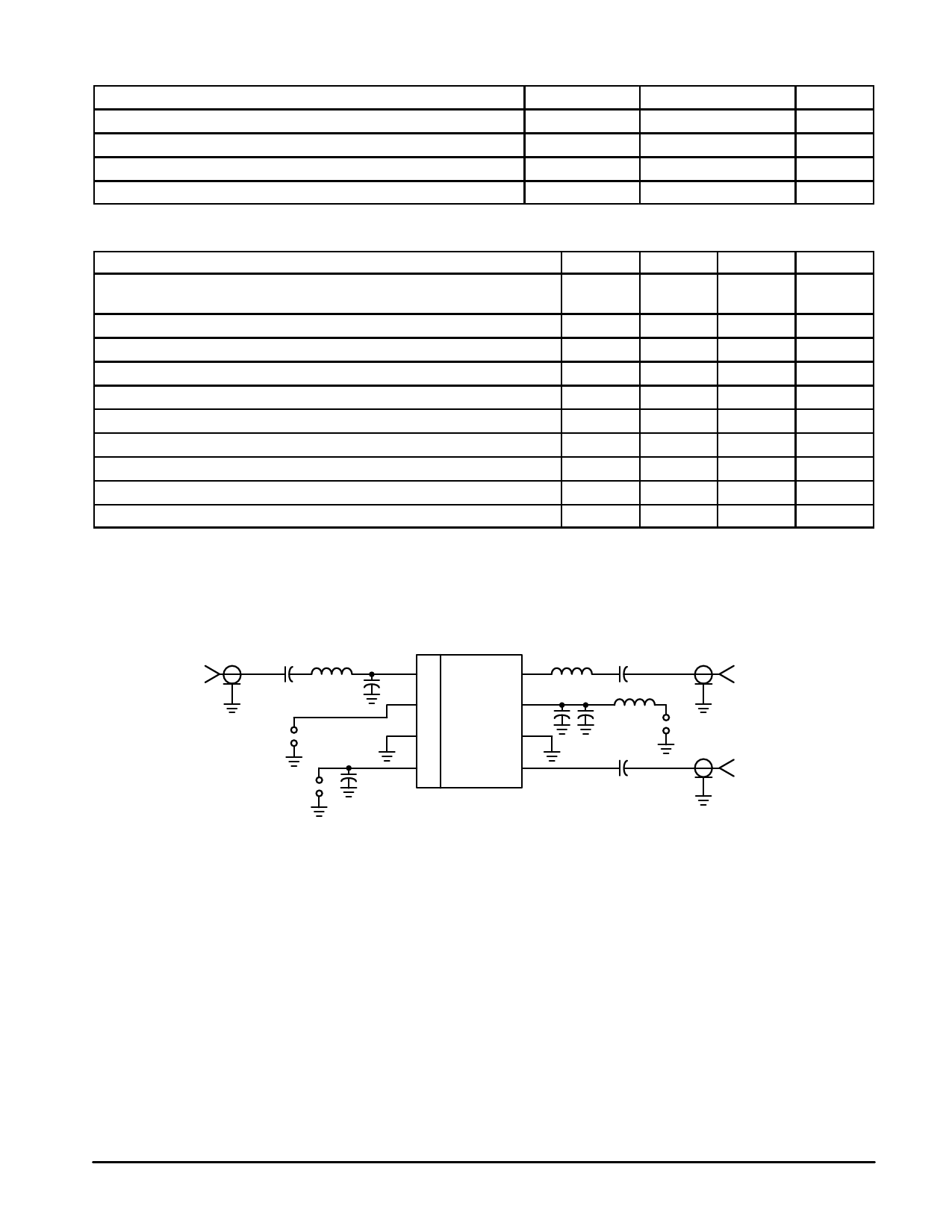
2. All Electrical Characteristics are measured in test circuit schematic as shown in Figure 1.
IF IN
C1 L1
50 Ω
1
C2
2
VRAMP*
+
–
3
4
ENABLE
+
–
C3
8
7
D.U.T.
6
5
L2
C5
C4
L3
C6
C7
+
– VCC
LO IN
50 Ω
RF OUT
50 Ω
C1, C3, C6 — 1000 pF Chip Capacitor
C2 — 6.8 pF Chip Capacitor
C4 — 3.9 pF Chip Capacitor
C5 — 100 pF Chip Capacitor
C7 — 5.6 pF Chip Capacitor
L1 — 270 nH Chip Inductor
L2 — 10 nH Chip Inductor
L3 — 390 nH Chip Inductor
RF Connectors — SMA Type
Board Material — Glass/Epoxy εr = 4.5,
Dielectric Thickness = 0.014″ (0.36 mm)
Figure 1. Test Circuit
Configuration
MRFIC2002
2
MOTOROLA RF DEVICE DATA
Share Link: 