UT62L2568LS-55LLI 查看數據表(PDF) - Utron Technology Inc
零件编号
产品描述 (功能)
比赛名单
UT62L2568LS-55LLI Datasheet PDF : 12 Pages
| |||
UTRON
Preliminary Rev. 0.1
UT62L2568(I)
256K X 8 BIT LOW POWER CMOS SRAM
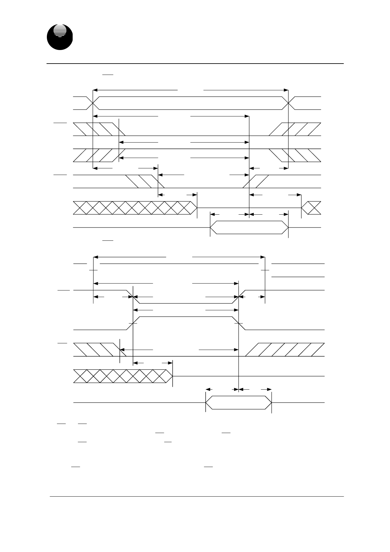
WRITE CYCLE 1 ( WE Controlled) (1,2,3,5)
t WC
Address
t AW
CE1
t CW1
CE2
t CW2
t AS
WE
t WP
t WR
Dout
Din
t WHZ
(4)
High-Z
t DW
t OW
(4)
t DH
Data Valid
WRITE CYCLE 2 ( CE 1 and CE2 Controlled) (1,2,5)
t WC
Address
CE1
t AS
CE2
t AW
t CW1
t CW2
t WR
WE
Dout
Din
t WP
t WHZ
High-Z
t DW
t DH
Data Valid
Notes :
1. WE or CE 1 must be HIGH or CE2 must be LOW during all address transitions.
2. A write occurs during the overlap of a low CE 1 , a high CE2 and a low WE .
3. During a WE controlled with write cycle with OE LOW, tWP must be greater than tWHZ+tDW to allow the I/O drivers to turn
off and data to be placed on the bus.
4. During this period, I/O pins are in the output state, and input signals must not be applied.
4. If the CE 1 LOW transition occurs simultaneously with or after WE LOW transition, the outputs remain in a high
Impedance state.
6. tOW and tWHZ are specified with CL=5pF. Transition is measured ±500mV from steady state.
UTRON TECHNOLOGY INC.
1F, No. 11, R&D Rd. II, Science-Based Industrial Park, Hsinchu, Taiwan, R. O. C.
TEL: 886-3-5777882 FAX: 886-3-5777919
6
P80082
Share Link: 