SN74LS42 查看數據表(PDF) - ON Semiconductor
零件编号
产品描述 (功能)
比赛名单
SN74LS42 Datasheet PDF : 7 Pages
| |||
SN74LS42
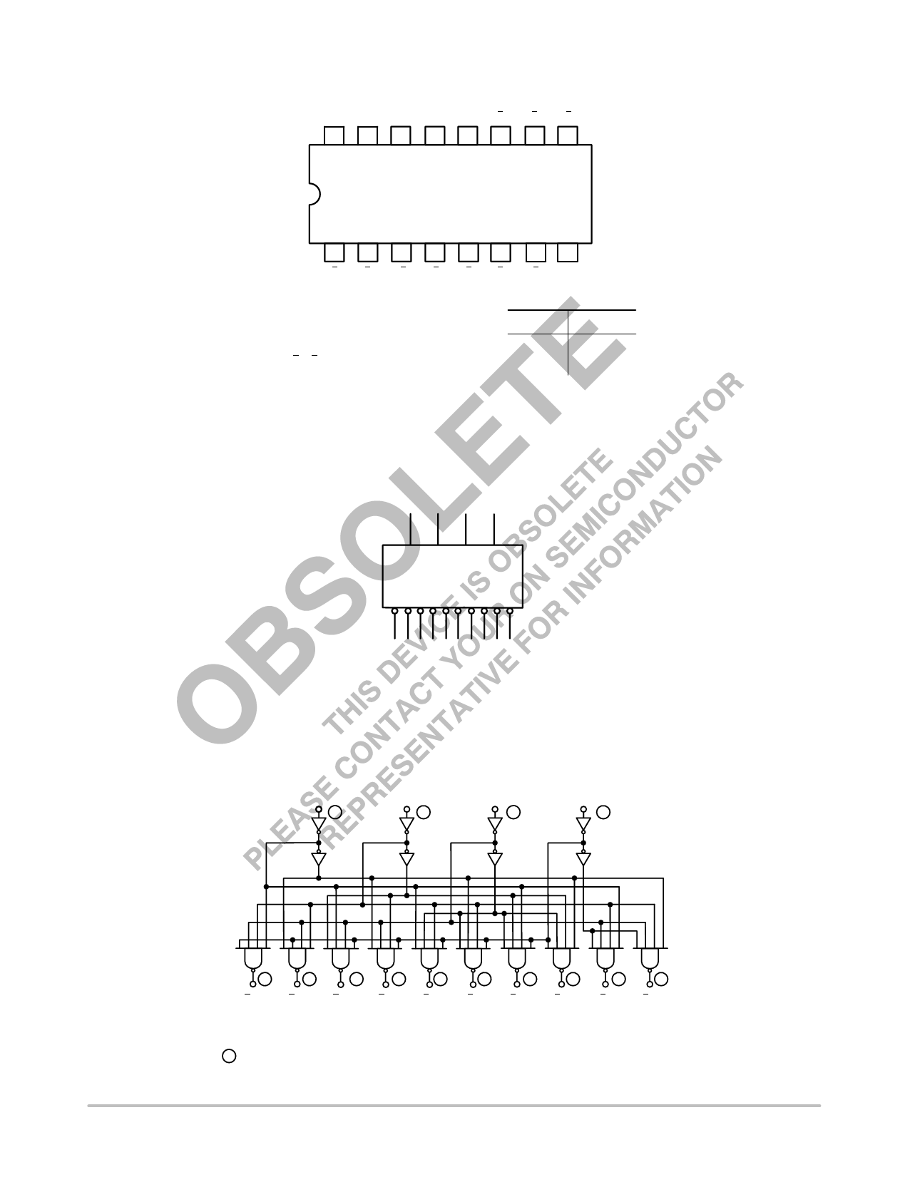
CONNECTION DIAGRAM DIP (TOP VIEW)
VCC A0 A1 A2 A3 9
16 15 14 13 12 11
1 2 3 4 56
0 1 2 3 45
87
10 9
78
6 GND
NOTE:
The Flatpak version
has the same pinouts
(Connection Diagram)
as the Dual In-Line
Package.
PIN NAMES
A0 − A3
0 to 9
Address Inputs
Outputs, Active LOW
LOADING (Note a)
HIGH
LOW
0.5 U.L.
10 U.L.
0.25 U.L.
5 U.L.
NOTES:
a) 1 TTL Unit Load (U.L.) = 40 mA HIGH/1.6 mA LOW.
LOGIC SYMBOL
15 14 13 12
A0 A1 A2 A3
012345 6 7 89
1 2 3 4 5 6 7 9 10 11
VCC = PIN 16
GND = PIN 8
A0
15
LOGIC DIAGRAM
A1
14
A2
13
A3
12
1
2
3
4
5
6
7
9
10
11
0
1
2
3
4
5
6
7
8
9
VCC = PIN 16
GND = PIN 8
= PIN NUMBERS
http://onsemi.com
2
Share Link: 