MX102DW 查看數據表(PDF) - MX-COM Inc
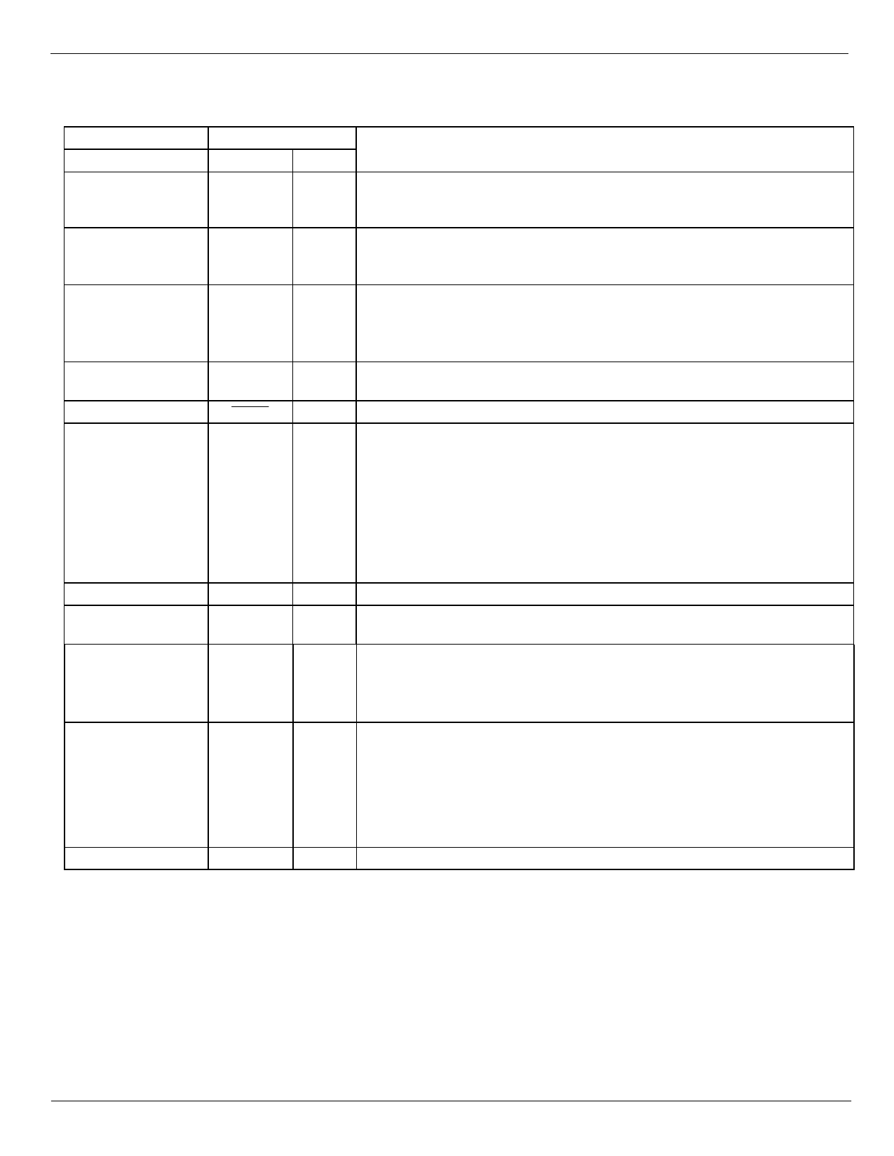
零件编号
产品描述 (功能)
比赛名单
MX102DW Datasheet PDF : 10 Pages
| |||
Autocorrelating Signal Processor
4
2. Signal List
MX102
Packages
DW/J
1
3
4
5
6
8
9
11
13
16
2, 7, 10, 12, 14, 15
Signal
Name Type
Signal In input
Signal
Bias
VDD
output
power
BUFCLK output
XTAL output
Xtal/Clock input
VSS
CLK ÷ 6
power
output
OUTPUT output
VDD
power
N/C
Description
The inverting input to the analog amplifier/comparator. Used with the
Signal Bias pin; external coupling components are required.
See Figure 2
The output of the analogue amplifier/comparator. Do not load this pin with
peripheral circuitry; there is no drive capacity for off-chip signaling. The
feedback resistor should be not less than 200kΩ. See Figure 2.
Positive supply rail. A single, stable power supply is required. Note that
this device has two VDD pins; this input is positioned to prevent cross-talk,
either or both may be connected to the host circuit's supply line. Do not
attempt to draw current from either VDD pin.
Buffered inverter oscillator digital output. May be used as test point to
align clock frequency or to drive other circuitry.
The output of the on-chip clock oscillator inverter.
The input to the on-chip clock oscillator inverter; this may be a Xtal,
resonator or clock pulse input. The selection of this frequency will affect
the operational input signal bandwidth (and output frequency) of this
device; refer to Table 4. Note that the choice of VDD will determine the
maximum Xtal/clock frequency and hence the maximum useable signal
input frequency. Operation of this microcircuit without an active Xtal or
clock input may cause device damage. A clock pulse input is fed directly
into this pin; Xtal/clock components are not required.
See Table 2.
Negative Supply
A squarewave output clock signal at the rate of Clock/6; provided for
peripheral and test purposes.
(fOUT = 4 x fSIGNAL IN). The auto-correlated output signal at four times
(x 4) the input signal (see Figure 3).
There is a time delay between input and output signals (see
Specifications).
Positive supply rail. A single, stable power supply is required.
Note that this device has two VDD pins; either or both may be connected
to the host circuit's supply line. Do not attempt to draw current from either
VDD pin.
The choice of VDD will determine the maximum Xtal/clock frequency and
hence the maximum useable signal input frequency (see Figure 4).
No internal connection. Leave open circuit
Table 1: Signal List
© 1997 MX•COM,INC.
www.mxcom.com Tele: 800 638 5577 910 744 5050 Fax: 910 744 5054
Doc.# 20480095.003
4800 Bethania Station road, Winston-Salem, NC 27105-1201 USA
All trademarks and service marks are held by their respective companies.
Share Link: 