LA9520V(2000) 查看數據表(PDF) - SANYO -> Panasonic
零件编号
产品描述 (功能)
比赛名单
LA9520V Datasheet PDF : 12 Pages
| |||
LA9520V
Continued from preceding page.
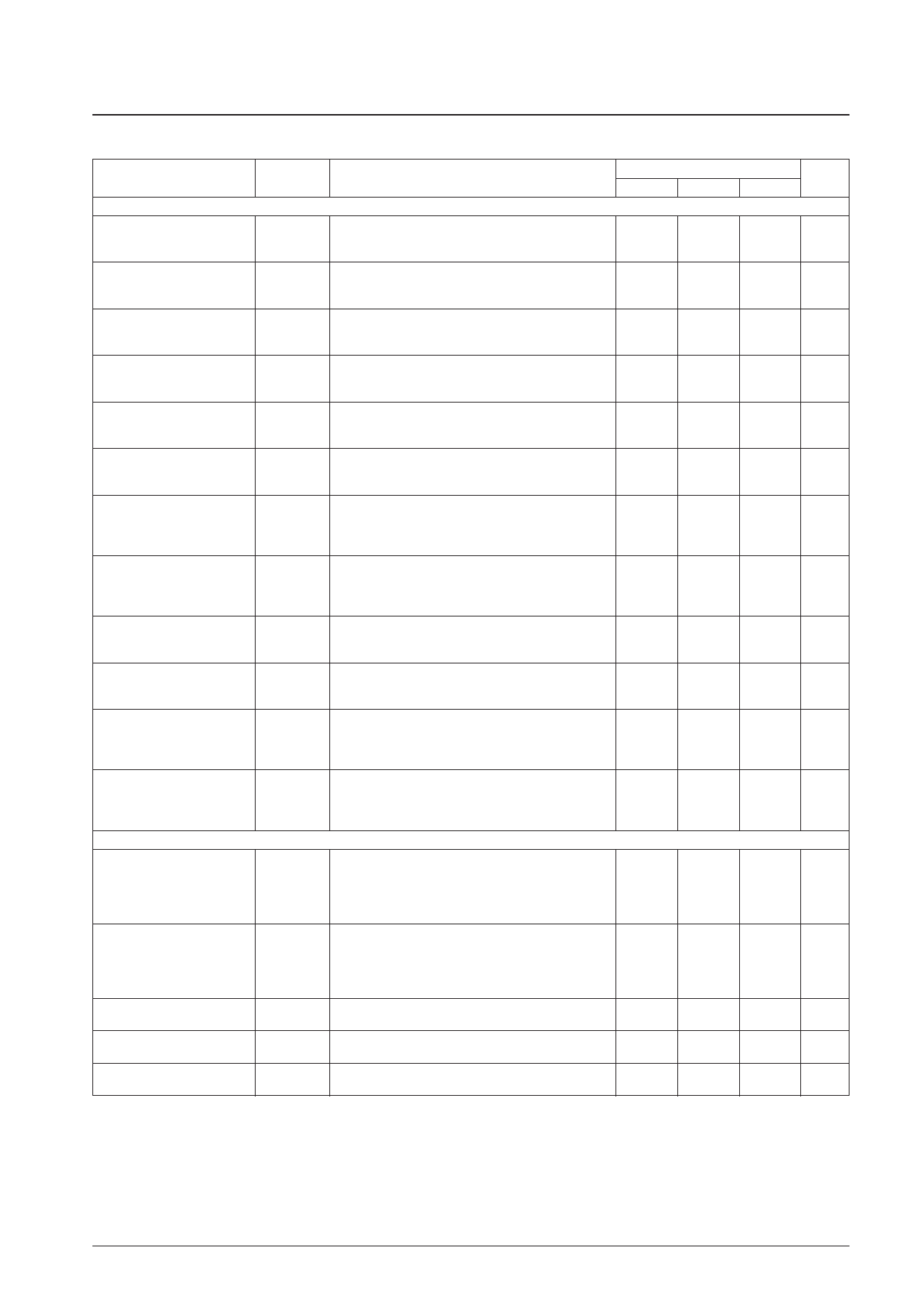
Parameter
Symbol
Conditions
[Audio Block] * Audio block initial output is adjusted with the pin 9 input.
Audio left channel
Output adjustment voltage
Audio right channel
Output adjustment voltage
Audio right channel
demodulator output
Audio left channel
demodulator output
Audio left channel amplifier
output
Audio right channel amplifier
output
Audio amplifier frequency
characteristics (L)
VacontL
For a 4.3 MHz, ∆f = ±22.5 kHz, fm = 400 Hz input,
the pin 14 adjustment voltage such that the pin 20 output
is 30 mV rms. VIN = 80 dBµ, Test pin: 14
VacontR
For a 4.8 MHz, ∆f = ±22.5 kHz, fm = 400 Hz input,
the pin 15 adjustment voltage such that the pin 21 output
is 30 mV rms. VIN = 80 dBµ, Test pin: 15
After reference output adjustment, the pin 21 demodulator
VdemR 75 kHz output when the input to pin 26 is 4.8 MHz ±75 kHz,
fm = 1 kHz, VIN = 80 dBµ, Test pin: 21
After reference output adjustment, the pin 20 demodulator
VdemL 75 kHz output when the input to pin 28 is 4.3 MHz ±75 kHz,
fm = 1 kHz, VIN = 80 dBµ, Test pin: 20
GvampL
The total amplifier gain (after output level adjustment)
from the pin 23 input to the pin 20 output.
VIN = 100 mVrms, f = 400 Hz., Test pin: 20
GvampR
The total amplifier gain (after output level adjustment)
from the pin 16 input to the pin 21 output.
VIN = 100 mVrms, f = 400 Hz., Test pin: 21
FA-AMP L
The frequency characteristics (after output level
adjustment) from pin 23 to pin 20. The frequency such
that the level is down –3 dB from the output reference at
f = 400 Hz, Test pin: 20
Audio amplifier frequency
characteristics (R)
FA-AMP R
The frequency characteristics (after output level
adjustment) from pin 16 to pin 21. The frequency such
that the level is down –3 dB from the output reference at
f = 400 Hz, Test pin: 21
Left channel total harmonic
distortion
Right channel total harmonic
distortion
Left channel output noise
voltage
Right channel output noise
voltage
[Muting Block]
THDL
THDR
VNLch
VNRch
The left channel distortion when a 4.3 MHz, ∆f = ±22.5 kHz,
fm = 1 kHz signal is input to pin 28.
VIN = 80 dBµ, Test pin: 20
The right channel distortion when a 4.8 MHz, ∆f = ±22.5 kHz,
fm = 1 kHz signal is input to pin 26.
VIN = 80 dBµ, Test pin: 21
With no modulation, the standard output reference
signal-to-noise ratio
IHFA filter, the LA9520V independent signal-to-noise ratio,
VIN = 80 dBµ, Test pin: 20
With no modulation, the standard output reference
signal-to-noise ratio
IHFA filter, the LA9520V independent signal-to-noise ratio,
VIN = 80 dBµ, Test pin: 21
Audio muting operating input
level 1
(Muting level adjustment
voltage)
Vmcont1
With no carrier input, the value of the voltage adjusted to
mute the audio output.
* With an external 30 dB amplifier connected to pin 9.
Rg = 4.7 kΩ
Test pin: 13
Video muting operating input
level 2
(Muting level adjustment
voltage)
Vmcont2
With no carrier input, the value of the voltage adjusted to
mute the audio output.
* With an external 30 dB amplifier connected to pin 9.
Rg = 4.7 kΩ
Test pin: 12
Muted signal output
Low level
VmuteL
The pin 29 output when the muting function is off.
Test pin: 29
Muted signal output
High level
VmuteH
The pin 29 output when the muting function is on.
Test pin: 29
Noise detection voltage level
VDET
The pin 11 voltage with no carrier input.
With an external 30 dB amplifier connected to pin 9.
min
0.05
0.05
0.6
0.6
15
15
45
45
0.05
0.05
VCC – 1
Ratings
typ
0.9
0.9
10
10
1.0
1.0
55
55
3.0
Unit
max
1.15 Vdc
1.15 Vdc
1.2 Vrms
1.2 Vrms
dB
dB
kHz
kHz
3
%
3
%
dB
dB
1.05 Vdc
1.05 Vdc
0.5 Vdc
Vdc
Vdc
No. 6469-3/12
Share Link: 