SPX2967T 查看數據表(PDF) - Signal Processing Technologies
零件编号
产品描述 (功能)
比赛名单
SPX2967T Datasheet PDF : 12 Pages
| |||
APPLICATIONS INFORMATION
The IC regulates an input voltage VI in the range of 5.5 V < VI <40 V to a nominal output voltage
of VQ= 5.0V. A reset signal is generated for an output voltage of VQ < VRT (typ. 4.5V). The reset
delay can be set with an external capacitor. The device has two logic inputs. A voltage of VE2 >4.0V
given to the E2-pin (e.g. by ignition) turns the device on. Depending on the voltage on pin E6 the
IC may be hold in active-state even if VE2 goes down to low level. This makes it simple to
implement a self-holding circuit without external components. When the device is turned off, the
output voltage drops to 0V and current consumption tends towards 0 µA.
DESIGN NOTES FOR EXTERNAL COMPONENTS
The input capacitor CI is necessary for compensation of line influences. The resonant circuit
consisting of lead inductance and input capacitance can be damped by a resistor of approxi-
mately 1Ω in series with CI . The output capacitor is necessary for the stability of the regulating
circuit. Stability is guaranteed at values of ≥ 22µF and an ESR of less than 3Ω within the operating
temperature range.
CIRCUIT DESCRIPTION
The control amplifier compares a reference voltage, which is kept highly accurate by resistance
adjustment, to a voltage that is proportional to the output voltage and drives the base of the series
transistor via a buffer. Saturation control as a function of the load current prevents and over-
saturation of the power element.
The reset output RO is in high state if the voltage on the delay capacitor CD greater than or equal
to VUD. The delay capacitance CD is charged with the current ID for output voltages greater than
the reset threshold VRT. If the output voltage gets lower than VRT a fast discharge of the delay
capacitor CD sets in and as soon as VCD gets lower than VLD the reset output RO is set to low-level.
The reset delay can be set within wide range by dimensioning the capacitance of the external
capacitor.
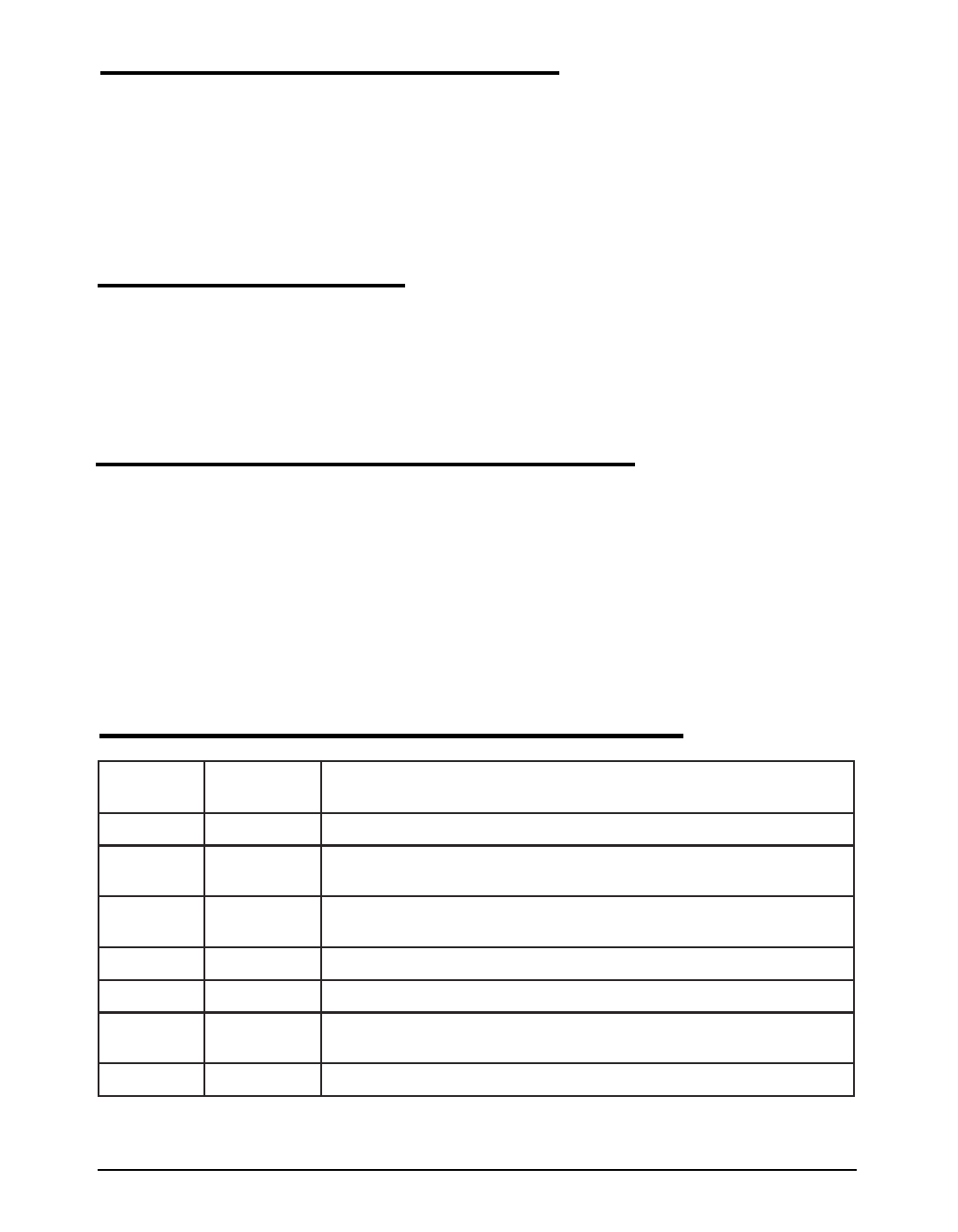
PIN DESCRIPTION
PIN
NUMBER
1
2
3
4
5
6
7
PIN NAME
I
E2
RO
GND
D
E6
Q
DESCRIPTION
Input; Block to GND directly at the IC with a ceramic capacitor.
Inhibit; Device is turned on by High signal on this pin; internal pulldown
resistor of 100kΩ
Reset Output; The open-collector output is internally linked to Q via a 30k
Ω resistor. Keep it open if not needed.
Ground; connected to rear of chip
Reset Delay; connect via capacitor to GND for setting delay
Hold; see truth table for function; this input is connected to output voltage
via a pull up resistor of 50kΩ
5V Output; block to GND with 22µF capacitor, ESR < 3Ω
Date: 8/23/04
SPX2967 400mA Low Dropout Voltage Regulator
2
© Copyright 2004 Sipex Corporation
Share Link: 