SS6612 查看數據表(PDF) - Silicon Standard Corp.
零件编号
产品描述 (功能)
比赛名单
SS6612
Silicon Standard Corp.

SS6612 Datasheet PDF : 16 Pages
| |||
SS6612
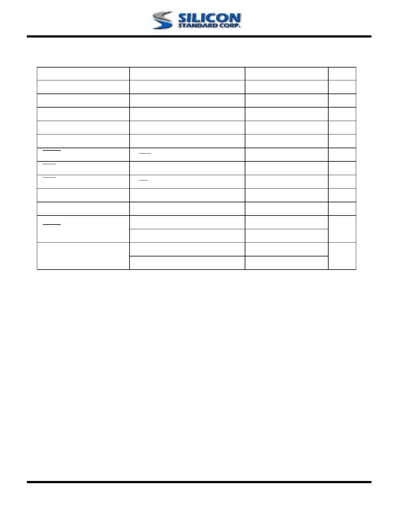
ELECTRICAL CHARACTERISTICS (Continued)
PARAMETER
LX Switch On-Time
LX Switch Off-Time
FB Input Current
LBI Input Current
CLSEL Input Current
SHDN Input Current
LBO Low Output Voltage
LBO Off Leakage Current
LBI Hystereisis
Damping Switch Resistance
SHDN Input Voltage
CLSEL Input Voltage
TEST CONDITIONS
VFB =1V , VOUT = 3.3V
VFB =1V , VOUT = 3.3V
VFB = 1.4V
VLBI = 1.4V
CLSEL = OUT
V SHDN = 0 or VOUT
VLBI = 0, ISINK = 1mA
VLBO = 5.5V, VLBI = 5.5V
VBATT = 2V
VIL
VIH
VIL
VIH
MIN. TYP. MAX. UNIT
2
4
7
µs
0.6
0.9
1.4
µs
0.03
50
nA
1
50
nA
1.4
3
µA
0.07
50
nA
0.2
0.4
µA
0.07
1
50
mV
50
100
Ω
0.8VOUT
0.2VOUT
V
0.8VOUT
0.2VOUT
V
Note 1: Start-up voltage operation is guaranteed without the addition of an external Schottky diode between the
input and output.
Note 2: Steady-state output current indicates that the device maintains output voltage regulation under load.
Note 3: Device is bootstrapped (power to the IC comes from OUT). This correlates directly with the actual bat-
tery supply.
Rev.2.02 12/06/2003
www.SiliconStandard.com
4 of 16
Share Link: