SS6652CNTB 查看數據表(PDF) - Silicon Standard Corp.
零件编号
产品描述 (功能)
比赛名单
SS6652CNTB Datasheet PDF : 6 Pages
| |||
n PIN DESCRIPTIONS
PIN 1: VIN - Input supply voltage (2.4V~7V)
PIN 2: VREF - Reference output (1.22V). Bypass
with a 0.047µF capacitor to GND.
Sourcing capability is guaranteed
to be greater than 250µA.
PIN 3: SHDN- Logic input to shutdown the chip.
>1.5V = normal operation,
GND = shutdown
In shutdown mode DLOW and
DHI pins are at high level.
PIN 4: FB
- Feedback signal input to sense
ground. Connecting a resistor R1
to VOUT and a resistor R2 to VREF
pin yields the output voltage:
VOUT = - (R1/R2 ) x VREF
PIN 5: GND - Power ground.
SS6652
PIN 6: DLOW - Driver sinking output. Connected
to DHI when using an external P-
channel MOSFET. When using an
external PNP bipolar transistor,
connect a resistor RB from this
pin to DHI. RB value depends on
VIN, inductor and PNP bipolar
transistor. By adjusting the RB
value, efficiency can be optimized.
PIN 7: DHI
- Driver sourcing output. Connect to
gate of the external P-channel
MOSFET or base of the PNP bi-
polar transistor.
PIN 8: CL
- Current-limit input. This pin
clamps the switch peak current to
prevent over-current damage to
the external switch.
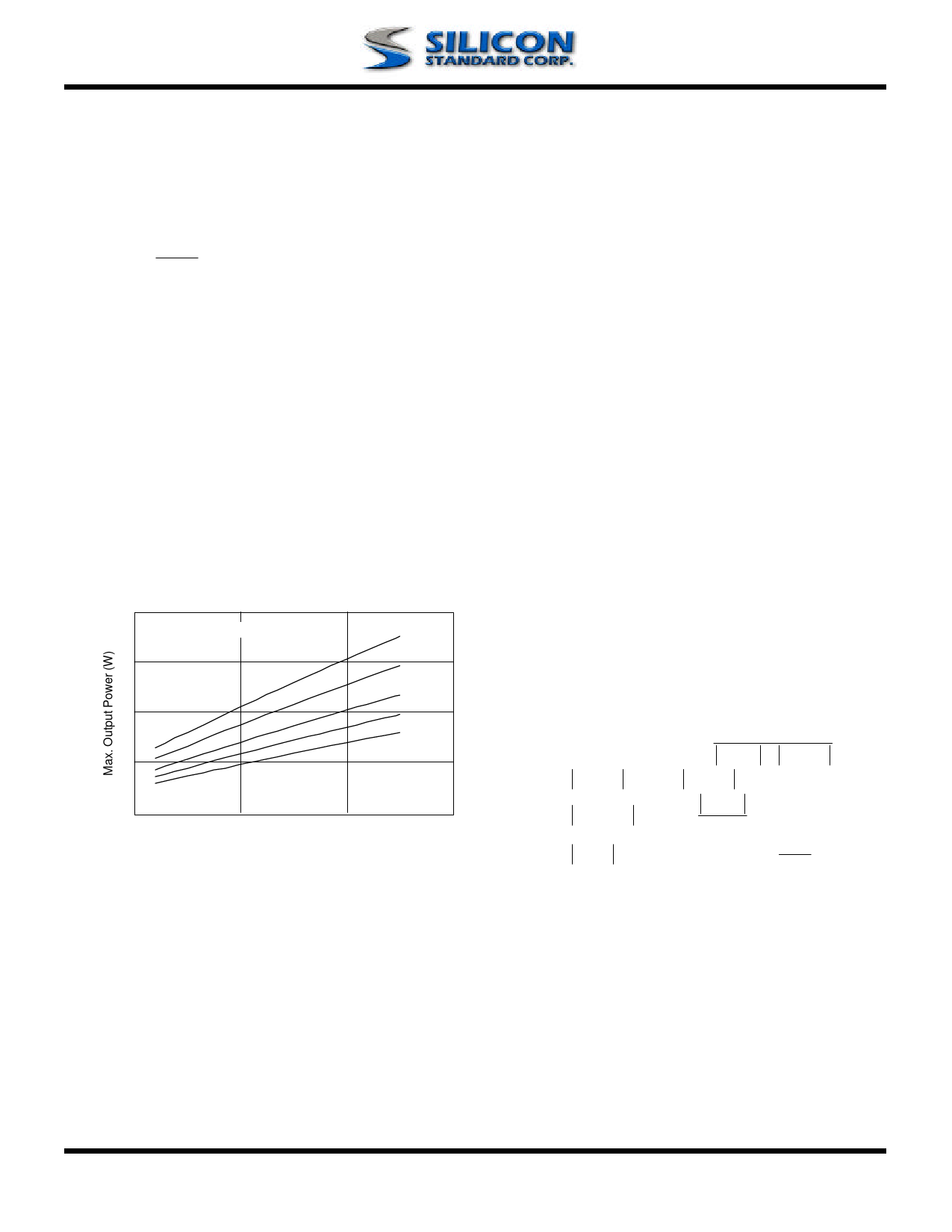
n APPLICATION INFORMATION
Max. Output Power vs VIN
0.8
Typical Application Circuit
100µH
0.6
120µH
150µH
0.4
180µH
220µH
Inductor Value
0.2
02
4
6
8
VIN (V)
The typical application circuit generates an adjustable
negative voltage for contrast bias of LCD displays. Ef-
ficiency and output power can be optimized by using
appropriate inductor and switch. The following formu-
lae provide a guideline for determining the optimal
component values:
L = (11.1 − 0.15 × VIN) ×
V IN
IOUT × V OUT
PNP : V CEO > VIN + V OUT
IC,MAX ≥ 200 × IOUT
VIN
V CE < 0. 4V at I C = 200 × IOUT
V IN
and β = 10
RB ≅ 3 x L x (VIN - 0.8)
where, VIN(V), VOUT(V), IOUT(A), L(µH), RB(Ω)
Rev.2.01 6/26/2003
www.SiliconStandard.com
4 of 6
Share Link: 