SSM9926O 查看數據表(PDF) - Silicon Standard Corp.
零件编号
产品描述 (功能)
比赛名单
SSM9926O Datasheet PDF : 6 Pages
| |||
SSM9926O
A
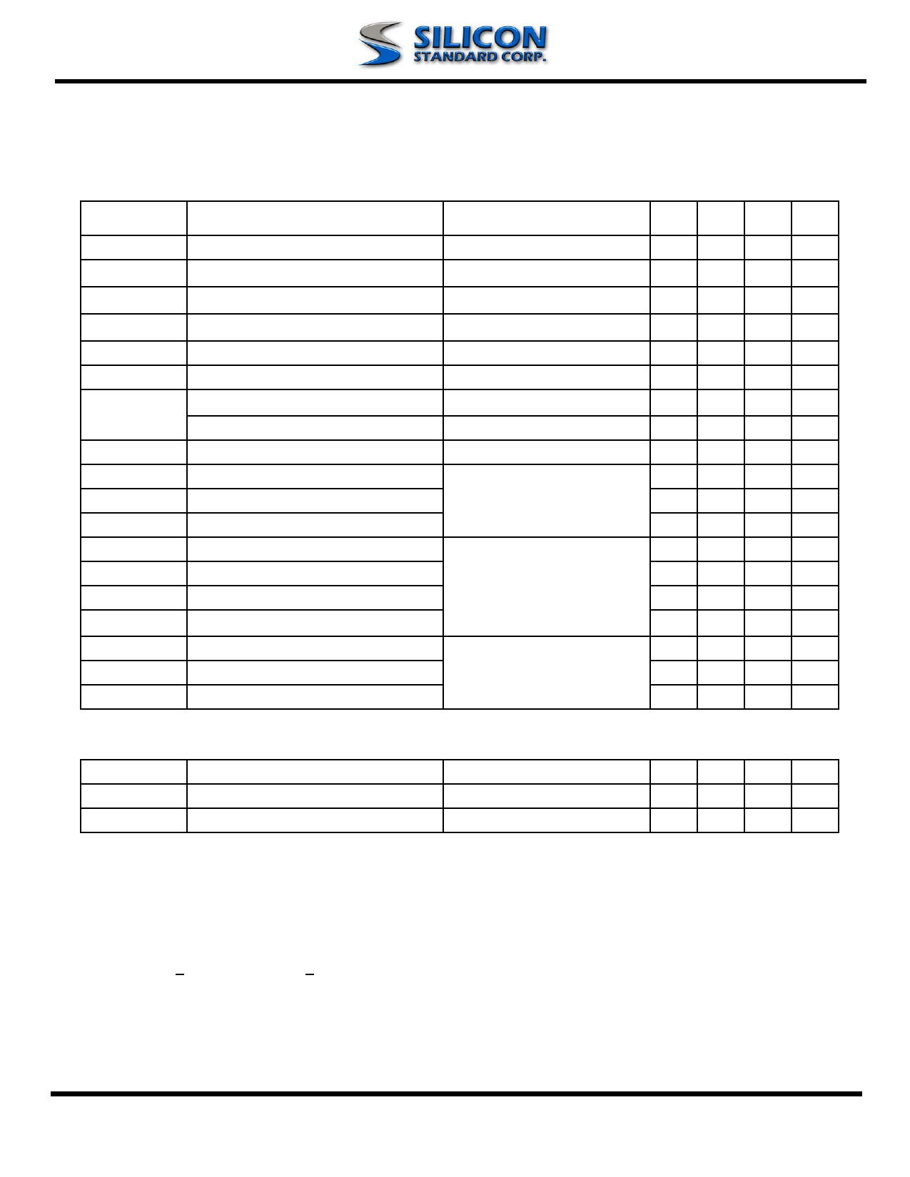
ELECTRICAL CHARACTERISTICS@Tj=25oC(unless otherwise specified)
Symbol
Parameter
Test Conditions
Min. Typ. Max. Units
BVDSS
ΔBVDSS/ΔTj
RDS(ON)
VGS(th)
gfs
IDSS
IGSS
Qg
Qgs
Qgd
td(on)
tr
td(off)
tf
Ciss
Coss
Crss
Drain-Source Breakdown Voltage
VGS=0V, ID=250uA
Breakdown Voltage Temperature Coefficient Reference to 25℃, ID=1mA
Static Drain-Source On-Resistance2 VGS=4.5V, ID=4A
VGS=2.5V, ID=2A
Gate Threshold Voltage
Forward Transconductance
Drain-Source Leakage Current (Tj=25oC)
Drain-Source Leakage Current (Tj=70oC)
Gate-Source Leakage
Total Gate Charge2
Gate-Source Charge
Gate-Drain ("Miller") Charge
Turn-on Delay Time2
Rise Time
Turn-off Delay Time
Fall Time
Input Capacitance
Output Capacitance
Reverse Transfer Capacitance
VDS=VGS, ID=250uA
VDS=10V, ID=4.6A
VDS=20V, VGS=0V
VDS=20V ,VGS=0V
VGS= ± 8V
ID=4.6A
VDS=20V
VGS=5V
VDS=10V
ID=1A
RG=3.3Ω,VGS=5V
RD=10Ω
VGS=0V
VDS=20V
f=1.0MHz
20 -
-
V
- 0.1 - V/℃
- 23 28 mΩ
-
- 40 mΩ
0.5 -
-
V
- 9.7 -
S
-
-
1 uA
-
- 25 uA
-
- ±100 nA
- 12.5 - nC
-
1
- nC
- 6.5 - nC
-
7
- ns
- 14.5 - ns
- 19 - ns
- 12 - ns
- 355 - pF
- 190 - pF
- 85 - pF
SOURCE-DRAIN DIODE
Symbol
Parameter
IS
Continuous Source Current ( Body Diode )
VSD
Forward On Voltage2
Test Conditions
VD=VG=0V,VS=1.2V
Tj=25℃,IS=1.25A,VGS=0V
Min. Typ. Max. Units
-
- 0.83 A
-
- 1.2 V
Notes:
1.Pulse width limited by Max. junction temperature.
2.Pulse width <300us , duty cycle <2%.
3.Surface mounted on 1 in2 copper pad of FR4 board ; 208℃/W when mounted on Min. copper pad.
03/11/2007 Rev.1.00
www.SiliconStandard.com
2
Share Link: 