TA8424 查看數據表(PDF) - Toshiba
零件编号
产品描述 (功能)
比赛名单
TA8424 Datasheet PDF : 12 Pages
| |||
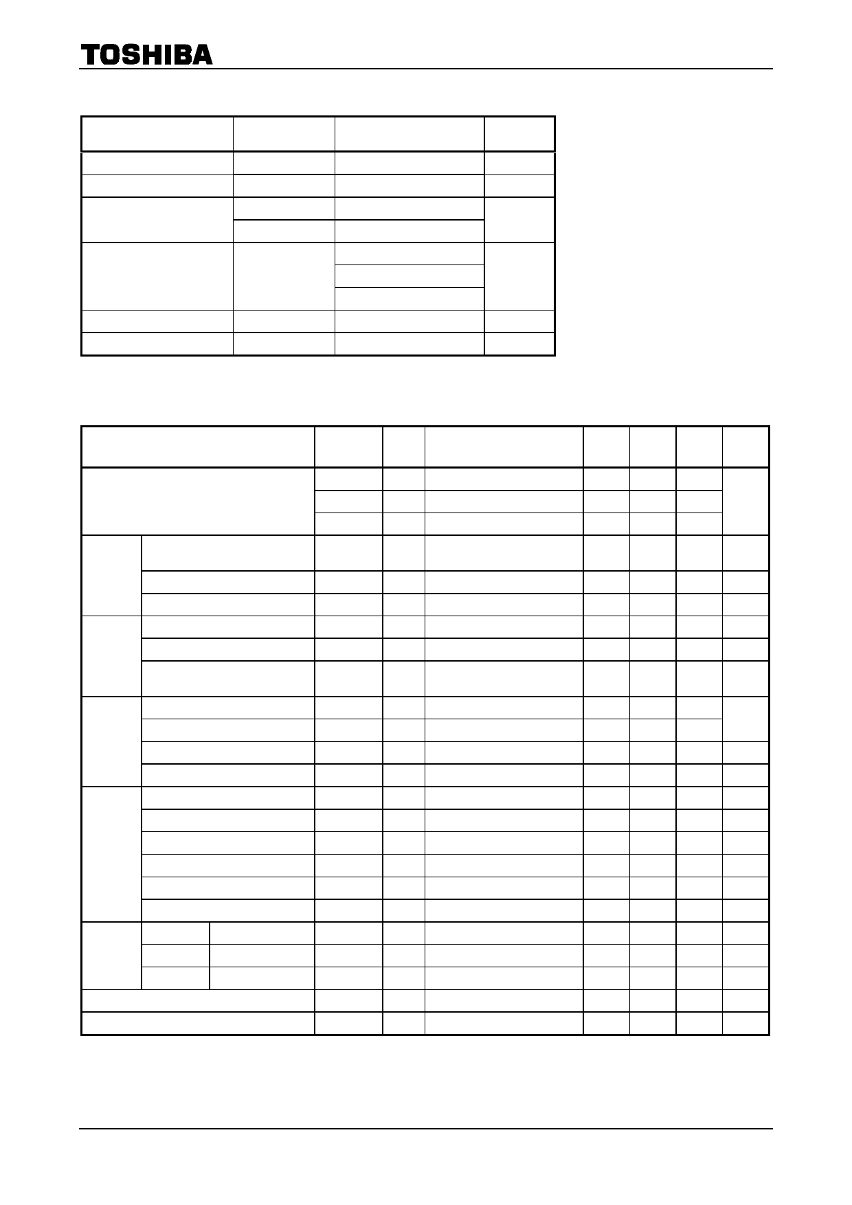
MAXIMUM RATINGS (Ta = 25°C)
CHARACTERISTIC
Supply Voltage
Output Current (Average)
FG Output Current
SYMBOL
VCC
IO (MAX.)
IFGO
IFGS
Power Dissipation
PD
Operating Temperature
Topr
Storage Temperature
Tstg
RATING
18
1.2
12
14
1.0
(Note 1)
3.2
(Note 2)
5.8
(Note 3)
−30~75
−55~150
TA8424F
UNIT
V
A
mA
W
Note 1: No Heat Sink
Note 2: 50 × 50 ×1mm Fe
°C
board, Mounting
°C
Note 3: Tc = 75°C
ELECTRICAL CHARACTERISTICS (VCC = 12 V, Ta = 25°C)
CHARACTERISTIC
Supply Current
Rotation
Control
Circuit
Position
Sensing
Circuit
Control Gain (VC → Out)
Input Current (VC)
Internal Reference−1
Common Mode Range
Input Current
Voltage Gain (Each Hall Input to
OUT)
SYMBOL
ICC1
ICC2
ICC3
GVCO
ICIN
Vref 1
CMRH
IH
GVHO
TEST
CIR−
CUIT
TEST CONDITION
― Output open, FRS = 2.5 V
― Output open, FRS = GND
― Output open, FRS = 5 V
―
VCC = 12 V,
VH = 50 mVp−p
― VC = GND (Sink current)
―
―
―
―
― VIH = 2.5 V
― VC = 5 V, VCC = 12 V
Upper Side Saturation
Output
Driver
Lower Side Saturation
Quiescent Voltage
Quiescent Voltage Difference
Open Loop Gain
Band Width
Output Voltage Swing
FG Amp
FGS Saturation
Internal Reference−2
Hysteresis Voltage
Rotation
Direction
Control
FWD
STOP
REVERSE
Operating Voltage
Operating Voltage
Operating Voltage
Regulator Output Voltage
Thermal Shutdown Operating Temperature
Vsat (U)
Vsat (L)
VOS
VOOF
GVFG
fFG
VFGO
Vsat (FGS)
Vref 2
VHYS
VFWD
VSTOP
VREV
VREG
TSD
― IO = 1.0 A
― IO = 1.0 A
― VC = 1.0 V
― Each output to output
― fFG = 1 kHz
―
―
― IFGO = 5 mA
― IFGS = 4 mA
―
―
―
―
―
―
―
―
―
―
― IH = 10 mA
―
―
MIN TYP. MAX UNIT
―
12.5
25
―
14
25
mA
―
14
25
7.5
13
18
dB
―
0.2
5
µA
2.15 2.30 2.45
V
1.5
―
5
V
―
0.2
3
µA
40
47
51
dB
―
1.2
1.9
V
―
0.7
1.5
5.0
5.5
7.0
V
―
25
50
mV
―
70
―
dB
DC
―
50
kHz
1.0
2.1
4
V
―
0.15 0.25
V
2.1
2.5
2.9
V
―
100 250 mV
4.0
―
VCC
V
1.9
―
3.1
V
0
―
1.3
V
4.7
5.1
5.5
V
150
―
―
°C
8
2001-06-13
Share Link: 