TC105 查看數據表(PDF) - Microchip Technology
零件编号
产品描述 (功能)
比赛名单
TC105 Datasheet PDF : 14 Pages
| |||
TC105
1.0 ELECTRICAL
CHARACTERISTICS
Absolute Maximum Ratings*
Voltage on VDD....................................... -0.3V to +12V
EXT Output Current ........................................±100mA
Voltage on VOUT, EXT,
SHDN Pins .....................................-0.3V to VDD +0.3V
Power Dissipation.............................................150mW
Operating Temperature Range............. -40°C to +85°C
Storage Temperature Range .............. -40°C to +125°C
*Stresses above those listed under "Absolute Maximum
Ratings" may cause permanent damage to the device. These
are stress ratings only and functional operation of the device
at these or any other conditions above those indicated in the
operation sections of the specifications is not implied.
Exposure to Absolute Maximum Rating conditions for
extended periods may affect device reliability.
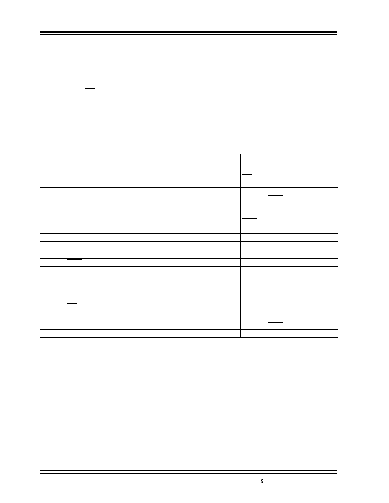
TC105 ELECTRICAL SPECIFICATIONS
Electrical Characteristics: Note 1, fOSC = 300 kHz; TA = 25°C, unless otherwise noted.
Symbol
Parameter
Min
Typ
Max Units
Test Conditions
VDD
Operating Supply Voltage
2.2
—
10.0
V
VDDMIN
Minimum Input Voltage
0.9
—
2.2
V EXT = High; No external components;
VOUT = 0V, SHDN = VIN
IDD
Operating Supply Current
—
57
102
µA No external components; VR = 3.0V, 3.3V
—
67
122
VOUT = 0V, SHDN = VIN VR = 5.0V
ISTBY
Standby Supply Current
—
15
27
µA No external components; VR = 3.0V, 3.3V
—
16
29
VOUT = SHDN = VIN
VR = 5.0V
ISHDN
Shutdown Supply Current
—
—
0.5
µA SHDN = GND
fOSC
Oscillator Frequency
255
300
345
kHz VIN = VOUT + 0.3V
VOUT
Output Voltage
VR x 0.975 VR VR x 1.025
Note 2
DTYMAX Maximum Duty Cycle (PWM Mode) 100
—
—
%
DTYPFM Duty Cycle (PFM Mode)
VIH
VIL
REXTH
SHDN Input Logic High
SHDN Input Logic Low
EXT ON Resistance to VDD
REXTL EXT ON Resistance to GND
η
Efficiency
15
25
35
% IOUT = 0mA
0.65
—
—
V VOUT = 0V, No external components
—
—
0.20
V VOUT = 0V, No external components
—
17
24
Ω No external components; VR = 3.0V
—
16
22
VR = 3.3V
—
12
17
VR = 5.0V
VOUT = SHDN = VIN, VEXT = (VIN – 0.4V)
—
15
20
Ω No external components; VR = 3.0V
—
14
19
VR = 3.3V
—
10
14
VR = 5.0V
VOUT = 0V, SHDN = VIN, VEXT = 0.4V
—
92
—
%
Note
1: VR = 3.0V, VIN = 4.5V, IOUT = 200mA
VR = 3.3V, VIN = 5.0V, IOUT = 220mA
VR = 5.0V, VIN = 7.5V, IOUT = 320mA
2: VR is the factory output voltage setting.
DS21349B-page 2
© 2002 Microchip Technology Inc.
Share Link: 