TC74ACT153 查看數據表(PDF) - Toshiba
零件编号
产品描述 (功能)
比赛名单
TC74ACT153 Datasheet PDF : 8 Pages
| |||
TC74ACT153P/F
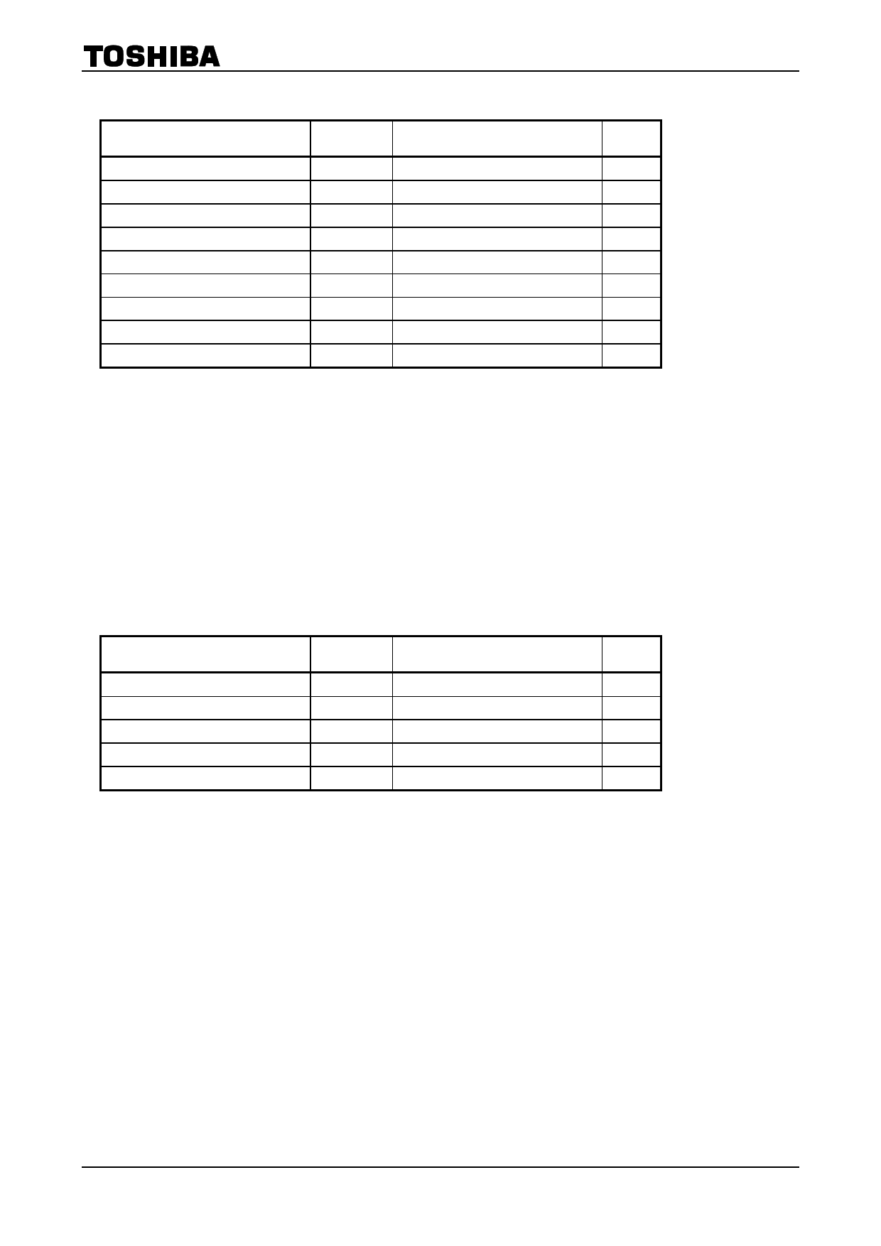
Absolute Maximum Ratings (Note 1)
Characteristics
Symbol
Rating
Unit
Supply voltage range
DC input voltage
DC output voltage
Input diode current
Output diode current
DC output current
DC VCC/ground current
Power dissipation
Storage temperature
VCC
VIN
VOUT
IIK
IOK
IOUT
ICC
PD
Tstg
−0.5 to 7.0
V
−0.5 to VCC + 0.5
V
−0.5 to VCC + 0.5
V
±20
mA
±50
mA
±50
mA
±100
mA
500 (DIP) (Note 2)/180 (SOP)
mW
−65 to 150
°C
Note 1:
Exceeding any of the absolute maximum ratings, even briefly, lead to deterioration in IC performance or
even destruction.
Using continuously under heavy loads (e.g. the application of high temperature/current/voltage and the
significant change in temperature, etc.) may cause this product to decrease in the reliability significantly
even if the operating conditions (i.e. operating temperature/current/voltage, etc.) are within the absolute
maximum ratings and the operating ranges.
Please design the appropriate reliability upon reviewing the Toshiba Semiconductor Reliability Handbook
(“Handling Precautions”/“Derating Concept and Methods”) and individual reliability data (i.e. reliability test
report and estimated failure rate, etc).
Note 2: 500 mW in the range of Ta = −40 to 65°C. From Ta = 65 to 85°C a derating factor of −10 mW/°C should be
applied up to 300 mW.
Operating Ranges (Note)
Characteristics
Symbol
Rating
Unit
Supply voltage
Input voltage
Output voltage
Operating temperature
Input rise and fall time
VCC
VIN
VOUT
Topr
dt/dV
4.5 to 5.5
0 to VCC
0 to VCC
−40 to 85
0 to 10
V
V
V
°C
ns/V
Note: The operating ranges must be maintained to ensure the normal operation of the device.
Unused inputs must be tied to either VCC or GND.
4
2012-02-29
Share Link: 