TDA7463A(2002) 查看數據表(PDF) - STMicroelectronics
零件编号
产品描述 (功能)
比赛名单
TDA7463A Datasheet PDF : 11 Pages
| |||
TDA7463A
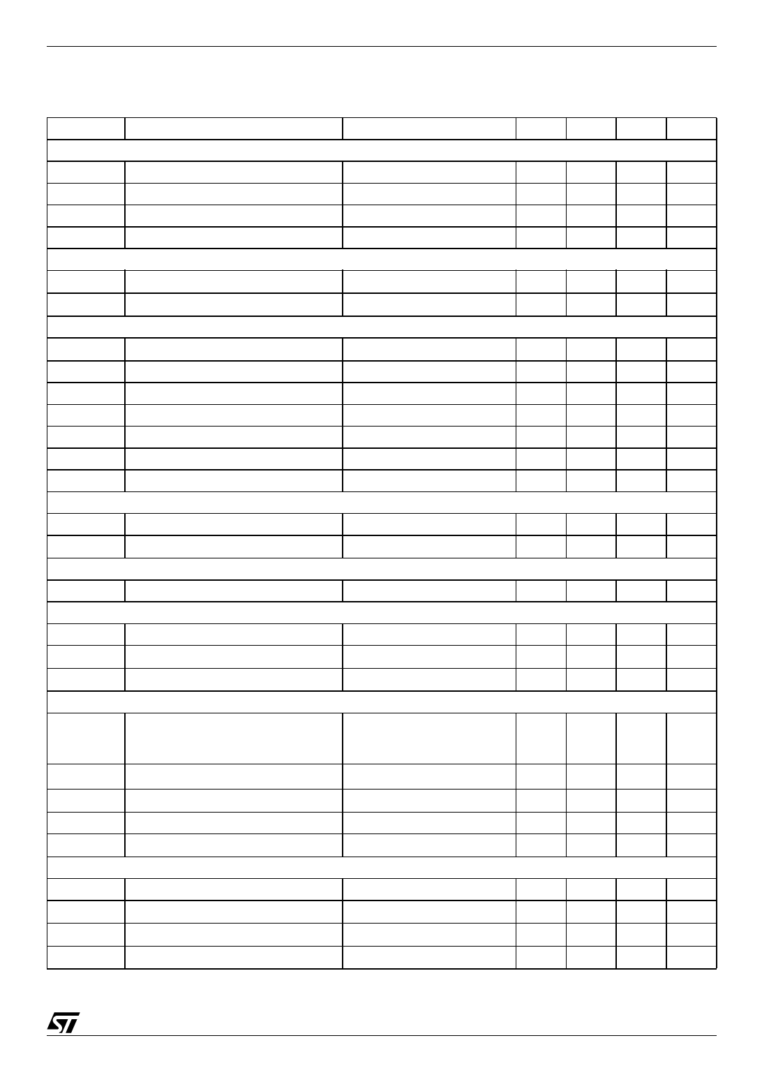
ELECTRICAL CHARACTERISTICS (refer to the test circuit Tamb = 25°C, VS =2.4V, RL= 10KΩ,
RG = 600Ω, all controls flat, unless otherwise specified)
Symbol
SUPPLY
Parameter
Test Condition
Min. Typ. Max. Unit
VS
IS
IST-BY
SVR
Supply Voltage
Supply Current
Stand-By Current
Ripple Rejection
1.8
2.4
3
4
50
70
INPUT STAGE
RIN
Input Resistance
VCL
Clipping Level
VOLUME CONTROL
CRANGE Control Range
AV MIN
Min Attenuation
AVMAX Max. Attenuation
ASTEP
Step Resolution
Amute
Mute Attenuation
A-10dB -10dB damping
G14dB 14dB gain
THD = 0.3%
35
50
65
0.2
63
-1
0
1
62
63
64
1
80
100
10
14
BASS CONTROL (1)
Gb
Control Range
RB
Internal Feedback Resistance
TREBLE CONTROL (1)
Gt
Control Range
Max. Boost/on
Max. Boost on
14
33.75 45 56.25
8
AUDIO OUTPUTS
VCLIP
Clipping Level
RL
Output Load Resistance
VDC
DC Voltage Level
d = 0.3%
0.2
10
0.8
GENERAL
ENO
Output Noise
Et
Total Tracking Error
S/N
Signal to Noise Ratio
SC
Channel Separation Left/Right
d
Distortion
Outout Muted
All gains = 0dB;
BW = 20Hz to 20KHz flat
All gains 0dB; VO = 0.1VRMS ;
AV = 0; VI = 0.1VRMS ;
5
8
0
1
80
80
0.1
BUS INPUT
VIL
Input Low Voltage
VIH
Input High Voltage
IIN
Input Current
VO
Output Voltage SDA
Acknowledge
VIN = 0.4V
IO = 1.6mA
0.5
1.9
-5
5
0.4
NOTE1:
1) BASS and TREBLE response: The center frequency and the response quality can be chosen by the external circuitry.
V
mA
µA
dB
KΩ
Vrms
dB
dB
dB
dB
dB
dB
dB
dB
KΩ
dB
VRMS
KΩ
V
µV
µV
dB
dB
dB
%
V
V
µA
V
3/11
Share Link: 