TDA8050 查看數據表(PDF) - Philips Electronics
零件编号
产品描述 (功能)
比赛名单
TDA8050 Datasheet PDF : 24 Pages
| |||
Philips Semiconductors
QPSK transmitter
Product specification
TDA8050
SYMBOL
PARAMETER
CONDITIONS
MIN. TYP. MAX. UNIT
Serial control clock
fclk
tsu
th(CLK)
td(strt)
td(stp)
clock frequency
input data to CLK set-up time
input data to CLK hold time
delay to rising clock edge
delay from last clock edge
see Fig.3
see Fig.3
see Fig.3
see Fig.3
−
330 −
kHz
−
2
−
µs
−
1
−
µs
−
3
−
µs
−
3
−
µs
Notes
1. All specification points of the output section and the overall circuit are measured after the 2 : 1 transformer
(siemens V944) connected with a load of 75 Ω.
2. Overall phase noise converter: Icp = 0.36 mA; fref = 12.5 kHz; VI(diff) = 100 mV; VO(diff) = 100 mV; VO = 55 dBmV;
DAC = 28; fi = 26.5 MHz.
3. Crystal oscillator; the crystal oscillator uses a 4, 2 or 1 MHz crystal in series with a capacitor. The crystal is serial
resonant with load a capacitance of 18 to 20 pF. The connection to VCC is preferred but can also be to GND.
Notes to the characteristics
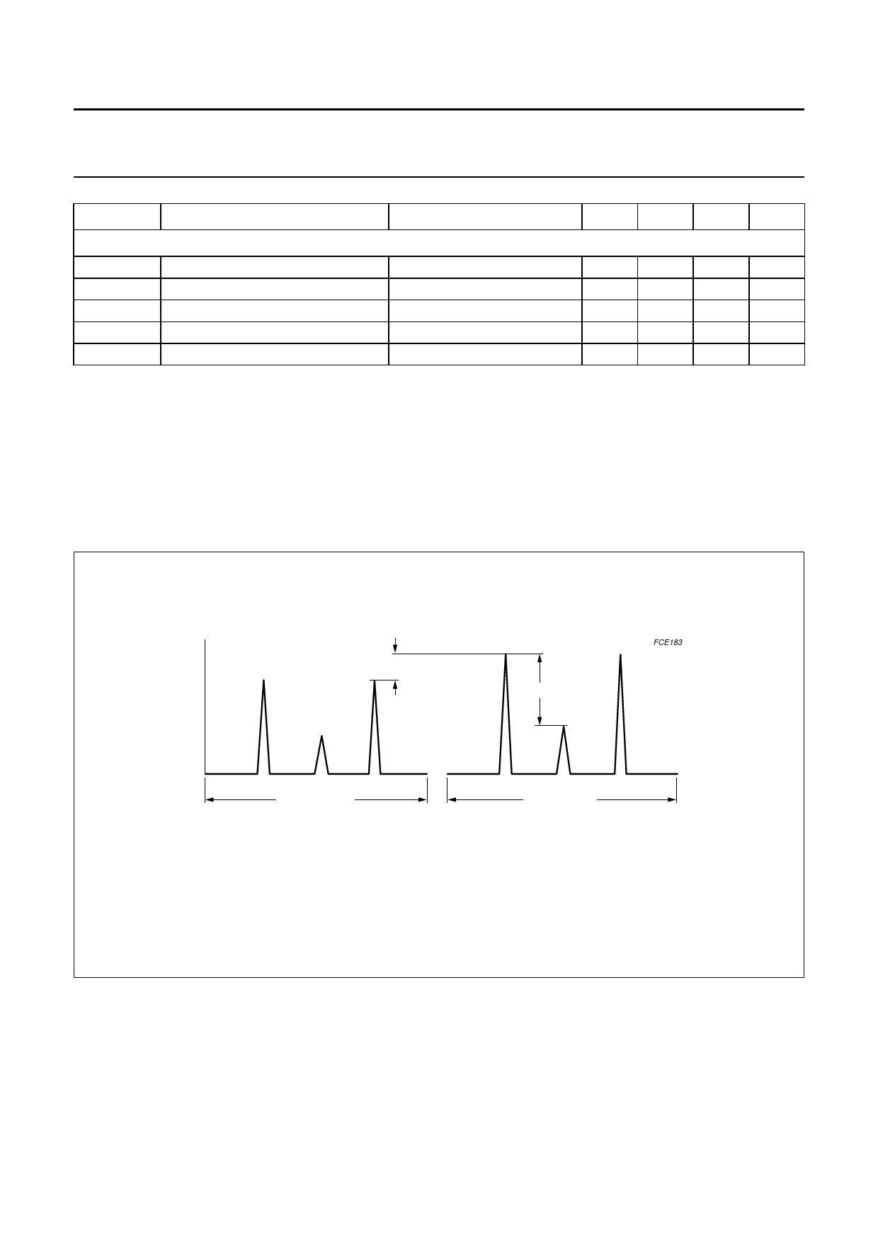
handbook, full pagewidth
IF_FILT
imbalance
LO(sup)
FCE183
measure 2 fi(Q)
measure 1 fi(I)
frequency
The amplitude imbalance and the LO suppression are measured in the spectrum of the signal measured at the output IF_FILT and are defined in the
following conditions:
Measure 1: I input frequency = 500 kHz. I input level = 400 mV (p-p) sine wave. Unused input as 0 V differential.
Measure 2: Q input frequency = 500 kHz. Q input level = 400 mV (p-p) sine wave. Unused input as 0 V differential.
Fig.3 Imbalance and LO suppression.
1999 Dec 14
9
Share Link: 