HT7660 查看數據表(PDF) - Holtek Semiconductor
零件编号
产品描述 (功能)
比赛名单
HT7660 Datasheet PDF : 10 Pages
| |||
HT7660
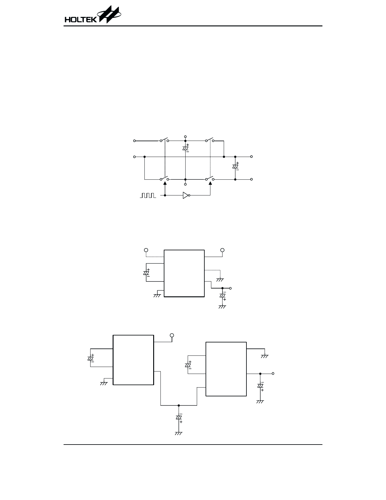
Functional Description
HT7660 needs only two external polarized electrolytic
capacitors to complete a negative voltage converter.
HT7660 has four MOS power switches: S1, S2, S3 and
S4. For the first half cycle, when S2 and S4 are open,
Capacitor C1 is charged to a voltage VDD through S1
and S3. During the second half cycle, when S1 and S3
are open, the charge on Capacitor C1 is shifted to Ca-
pacitor C2 through S2 and S4. Thereby, the voltage
across Capacitor C2 is VDD. Because the positive termi-
nal of C2 is connected to VSS, we get a -VDD voltage at
VOUT pin.
For high voltage operation, the LV pin is left floating to
enable the voltage regulator. This can reduce the cur-
rent consumption of the RC oscillator, and thus get a
fixed switching frequency fOSC with high voltage range.
For low voltage operation, the LV pin is connected to
VSS to bypass the voltage regulator of which inherent
voltage drop can degrade the operation at low voltages.
A capacitor may be connected between VDD and pin
OSC to lower the switching fOSC, and an external clock
may be added to replace the built-in RC oscillator.
V DD
S1
CAP+ S2
C1
V SS
S3
S4
CAP-
V SS
C2
V O UT= - V DD
The operating mode of HT7660
Application Circuits
Simple Negative Voltage Converter
V DD
10m.
V DD
1 BO O ST
2 CAP+
VDD 8
6
LV
4 CAP-
3 VSS
VO UT
H T7660
5
10m.
V O U T = -V D D
Simple Voltage Multiplier
2 CAP+
8
VDD
10m.
4 CAP-
3 VSS
5
VO UT
H T7660
V DD
10m.
10m.
2 CAP+
8
VDD
4 CAP-
3 VSS
5
VO UT
H T7660
V O UT= - 2 V DD
10m.
Rev. 1.10
3
January 21, 2003
Share Link: 