ADG728(2000) 查看數據表(PDF) - Analog Devices
零件编号
产品描述 (功能)
比赛名单
ADG728 Datasheet PDF : 12 Pages
| |||
ADG728/ADG729
MULTIPLE DEVICES ON ONE BUS
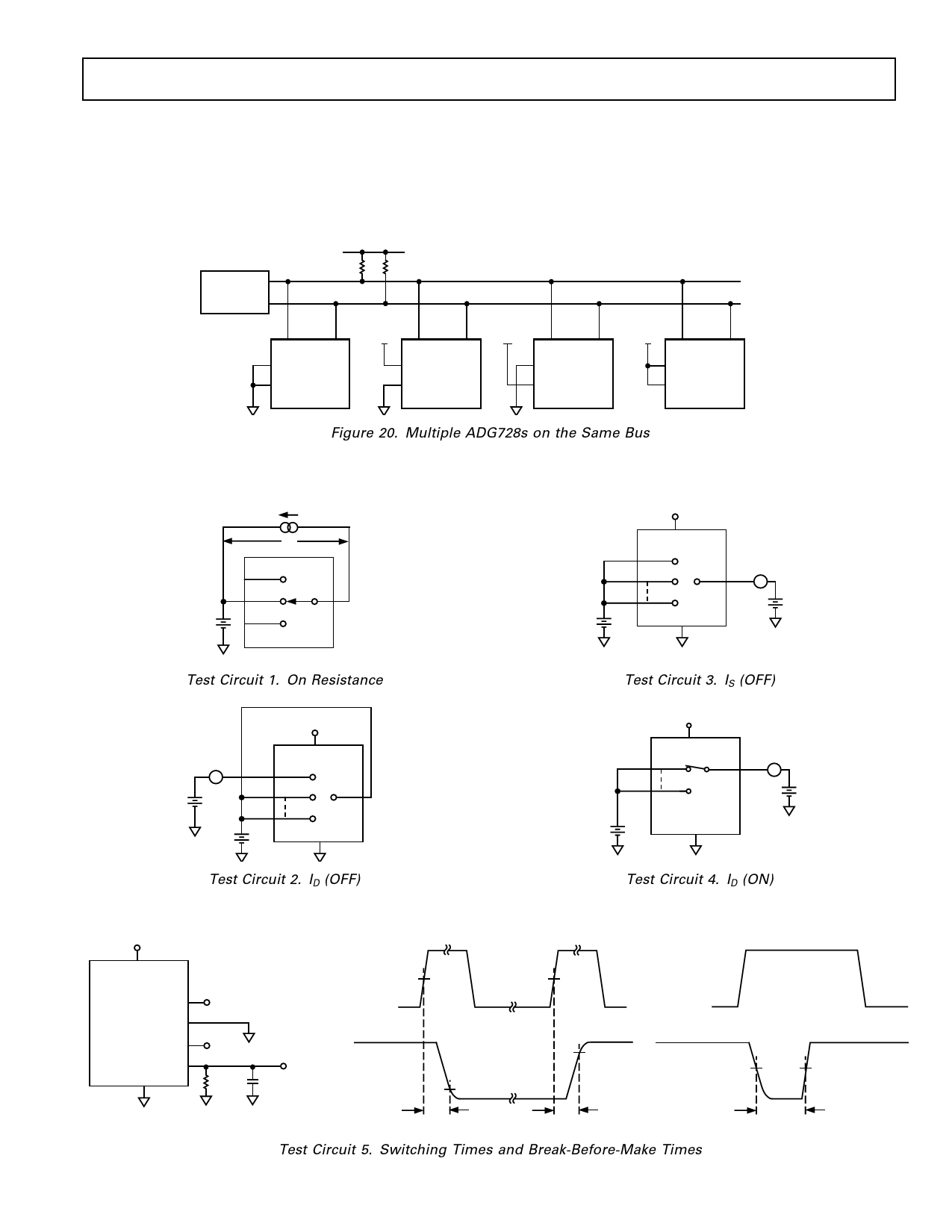
Figure 20 shows four ADG728s devices on the same serial bus.
Each has a different slave address since the state of their A0 and
A1 pins is different. This allows each Matrix Switch to be writ-
ten to or read from independently. Because the ADG729 has a
different address to the ADG728, it would be possible for four
of each of these devices to be connected to the same bus.
MASTER
+5V
RP
RP
SDA
SCL
SDA
SCL
A1
A0
ADG728
VDD
SDA
A1
SCL
A0
ADG728
VDD
SDA
A1
SCL
A0
ADG728
VDD
SDA
A1
SCL
A0
ADG728
Figure 20. Multiple ADG728s on the Same Bus
TEST CIRCUITS
IDS
V1
S
D
VS
RON = V1/IDS
Test Circuit 1. On Resistance
IS (OFF)
S1
A
S2
VS
S8
VD
VDD
VDD
D
GND
S1
S2
S8
VS
VDD
VDD
GND
ID (OFF)
D
A
VD
Test Circuit 3. IS (OFF)
VDD
VDD
S1
S8
ID (ON)
D
A
VD
VS
GND
Test Circuit 2. ID (OFF)
Test Circuit 4. ID (ON)
VDD
VDD
ADG728*
S1
S2 THRU S7
S8
D
GND
VS1
VS8
RL
300⍀
SCL
VOUT
CL
35pF
VS1
VOUT
50%
50%
90%
90%
VS1 = VS8
VOUT
* SIMILAR CONNECTION FOR ADG729
tOFF
tON
Test Circuit 5. Switching Times and Break-Before-Make Times
80%
80%
tOPEN
REV. A
–11–
Share Link: 