ADG714(Rev0) 查看數據表(PDF) - Analog Devices
零件编号
产品描述 (功能)
比赛名单
ADG714 Datasheet PDF : 16 Pages
| |||
ABSOLUTE MAXIMUM RATINGS1
(TA = 25°C unless otherwise noted)
VDD to VSS . . . . . . . . . . . . . . . . . . . . . . . . . . . . . . . . . . . . . 7 V
VDD to GND . . . . . . . . . . . . . . . . . . . . . . . . . . –0.3 V to +7 V
VSS to GND . . . . . . . . . . . . . . . . . . . . . . . . . . +0.3 V to –3.5 V
Analog Inputs2 . . . . . . . . . . . . . . . VSS – 0.3 V to VDD + 0.3 V
or 30 mA, Whichever Occurs First
Digital Inputs2 . . . . . . . . . . . . . . . . . . . –0.3 V to VDD + 0.3 V
or 30 mA, Whichever Occurs First
Peak Current, S or D . . . . . . . . . . . . . . . . . . . . . . . . . .100 mA
(Pulsed at 1 ms, 10% Duty Cycle Max)
Continuous Current, S or D . . . . . . . . . . . . . . . . . . . . 30 mA
Operating Temperature Range
Industrial (B Version) . . . . . . . . . . . . . . . . –40°C to +85°C
Storage Temperature Range . . . . . . . . . . . . –65°C to +150°C
Junction Temperature . . . . . . . . . . . . . . . . . . . . . . . . . . 150°C
ADG714/ADG715
TSSOP Package
θJA Thermal Impedance . . . . . . . . . . . . . . . . . . . . 128°C/W
θJC Thermal Impedance . . . . . . . . . . . . . . . . . . . . . 42°C/W
Lead Temperature, Soldering
Vapor Phase (60 sec) . . . . . . . . . . . . . . . . . . . . . . . . . 215°C
Infrared (15 sec) . . . . . . . . . . . . . . . . . . . . . . . . . . . . . 220°C
NOTES
1Stresses above those listed under Absolute Maximum Ratings may cause perma-
nent damage to the device. This is a stress rating only; functional operation of the
device at these or any other conditions above those listed in the operational
sections of this specification is not implied. Exposure to absolute maximum rating
conditions for extended periods may affect device reliability. Only one absolute
maximum rating may be applied at any one time.
2Overvoltages at IN, S, or D will be clamped by internal diodes. Current should be
limited to the maximum ratings given.
CAUTION
ESD (electrostatic discharge) sensitive device. Electrostatic charges as high as 4000 V readily
accumulate on the human body and test equipment and can discharge without detection. Although
the ADG714/ADG715 feature proprietary ESD protection circuitry, permanent damage may occur
on devices subjected to high-energy electrostatic discharges. Therefore, proper ESD precautions
are recommended to avoid performance degradation or loss of functionality.
WARNING!
ESD SENSITIVE DEVICE
Model
ADG714BRU
ADG715BRU
Temperature Range
–40°C to +85°C
–40°C to +85°C
ORDERING GUIDE
Interface
SPI/QSPI/MICROWIRE
I2C-Compatible
Package Description
TSSOP
TSSOP
Package Option
RU-24
RU-24
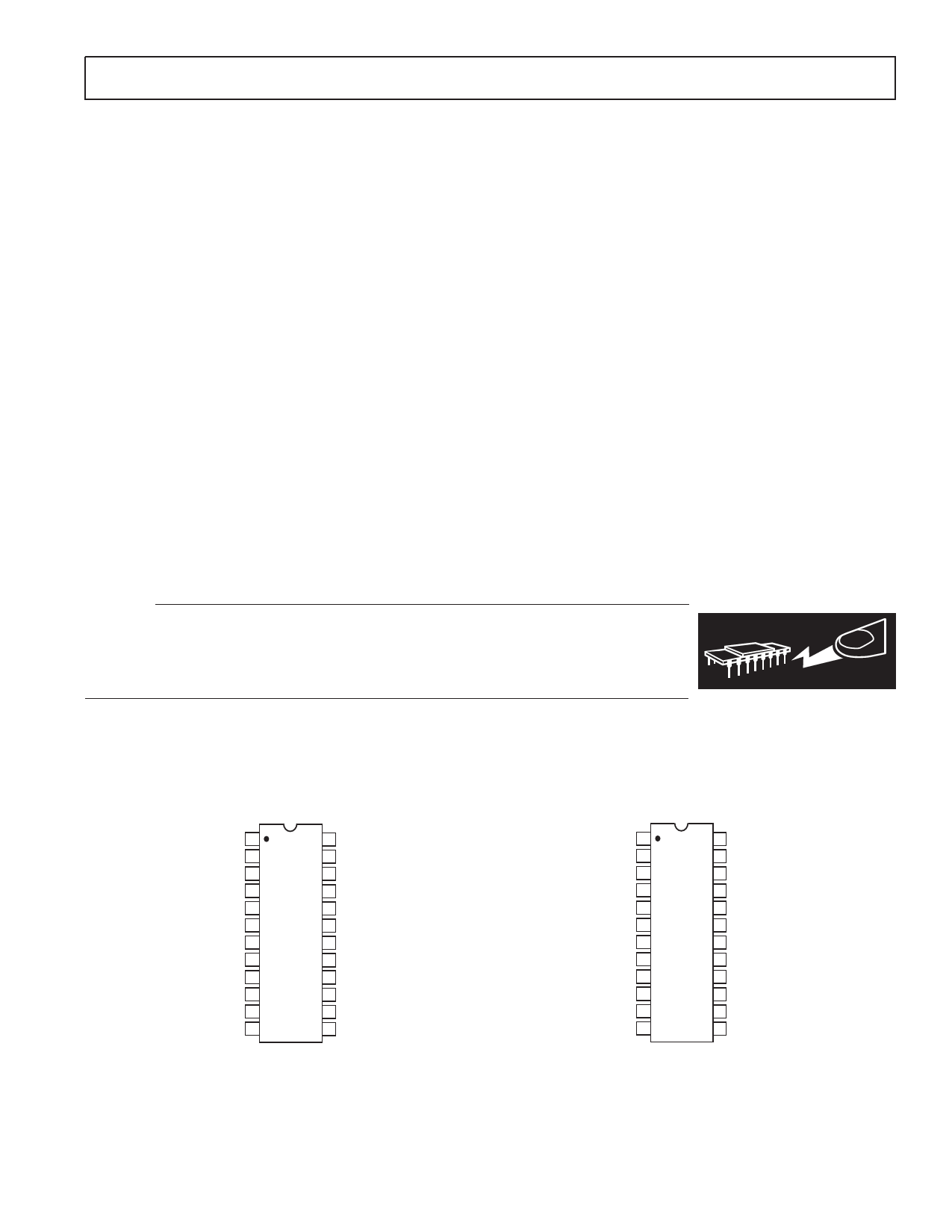
PIN CONFIGURATIONS
24-Lead TSSOP
SCLK 1
24 SYNC
VDD 2
DIN 3
23 RESET
22 DOUT
GND
S1
D1
S2
4
21 VSS
5 ADG714 20 S8
6 TOP VIEW 19 D8
7 (Not to Scale) 18 S7
D2 8
17 D7
S3 9
16 S6
D3 10
15 D6
S4 11
14 S5
D4 12
13 D5
SCL 1
24 A0
VDD 2
SDA 3
23 RESET
22 A1
GND
S1
D1
S2
4
21 VSS
5 ADG715 20 S8
6 TOP VIEW 19 D8
7 (Not to Scale) 18 S7
D2 8
17 D7
S3 9
16 S6
D3 10
15 D6
S4 11
14 S5
D4 12
13 D5
REV. 0
–7–
Share Link: 