ST70136G 查看數據表(PDF) - STMicroelectronics
零件编号
产品描述 (功能)
比赛名单
ST70136G Datasheet PDF : 24 Pages
| |||
ST70136
4.7.1.3 - Special Features Configuration
This register is located at the address “010” and is used to configure different blocks.
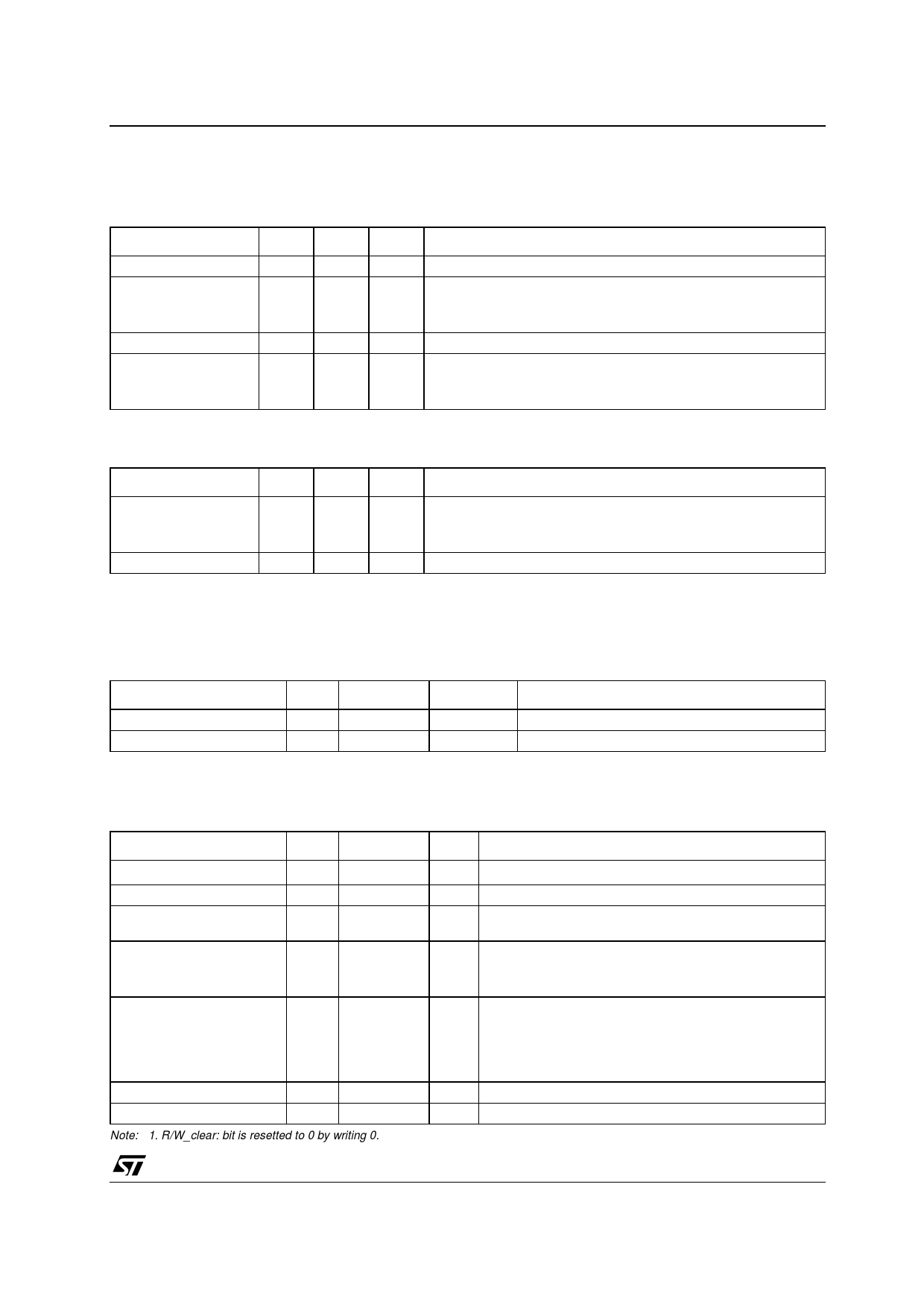
Table 4 : Adsl Configuration (address [b2:b0]=”010”)
Name
Reserved
VCO-DAC
Other
FVCXO
Pos.
14.13
12
Type
R/W
R/W
11.4 R/W
3
R/W
Def.
00 Reserved
1 Enable the VCO DAC
0..0 Reserved
0 Filtered VCXO output
Description
1: enabled
0: disabled
1 : filtered
0 : not filtered
4.7.1.4 - VCXO Control
Table 5 : VCXO DAC Value (address [b2:b0]=”011”)
Name
DAC value
Others
pos.
14..7
type
R/W
def.
80H 8 bits for VCO DAC.
6..3 R/W 0000 Reserved
Description
0...0 = min. current
1...1 = max current.
4.7.1.5 - Test Only Registers
They are presently located at address “100” to “101”.
4.7.1.6 - Tone Detection Threshold Setting Register
Table 6 : Tone Detection Threshold Setting Register (address [b2:b0]=”110”)
Name
Threshold Level
Reserved
Pos.
14..5
4.3
Type
R/W
R/W
Def.
Description
1000000000 Set the threshold of the tone detector
00
Reserved
4.7.1.7 - Status Register & tone detector
This register can be used in the case of read / write registers.
Table 7 : Status & Tone Detector Register (address [b2:b0]=”111”)
Name
Receiver Clip indicator
Transceiver Clip indicator
Sleeping Mode
Tone Detector
Pos.
14
13
12
Type
R/W_clear 1
R/W_clear
R/W
11
R/W
Debug Mode
10
R/W
Software Reset
9
R/W
Reserved
8..3
R/W
Note: 1. R/W_clear: bit is resetted to 0 by writing 0.
Def.
Description
0 1: Receive Clipping occurred
0 1: Transmit Clipping occurred
0 0: disable tone detector in power down
1: enable tone detector in power down
0 Tone detector frequency setting
0: standard ADSL (tone 40)
1: ADSL over ISDN (tone 72)
0 When in normal mode “0” the CTRLOUT pin is in HIZ
and don’t care for R/W and the control access register
are always writing operation whatever on R/W pin.
When in debug mode “1” the CTRLOUT and R/W pins
are operating as defined in pin description chapter.
0 When set all registers are set to their default value
0..0 Reserved
11/24
Share Link: 