CMX639 查看數據表(PDF) - CML Microsystems Plc
零件编号
产品描述 (功能)
比赛名单
CMX639 Datasheet PDF : 16 Pages
| |||
CVSD Codec
CMX639
P6
22-pin
PDIP
15
16
17
18
19
20
21
22
E2
24-pin
TSSOP
16
17
18
19
20
21
22
23
24
D4
16-pin
SOIC
10
Not
present
11
12
13
14
15
16
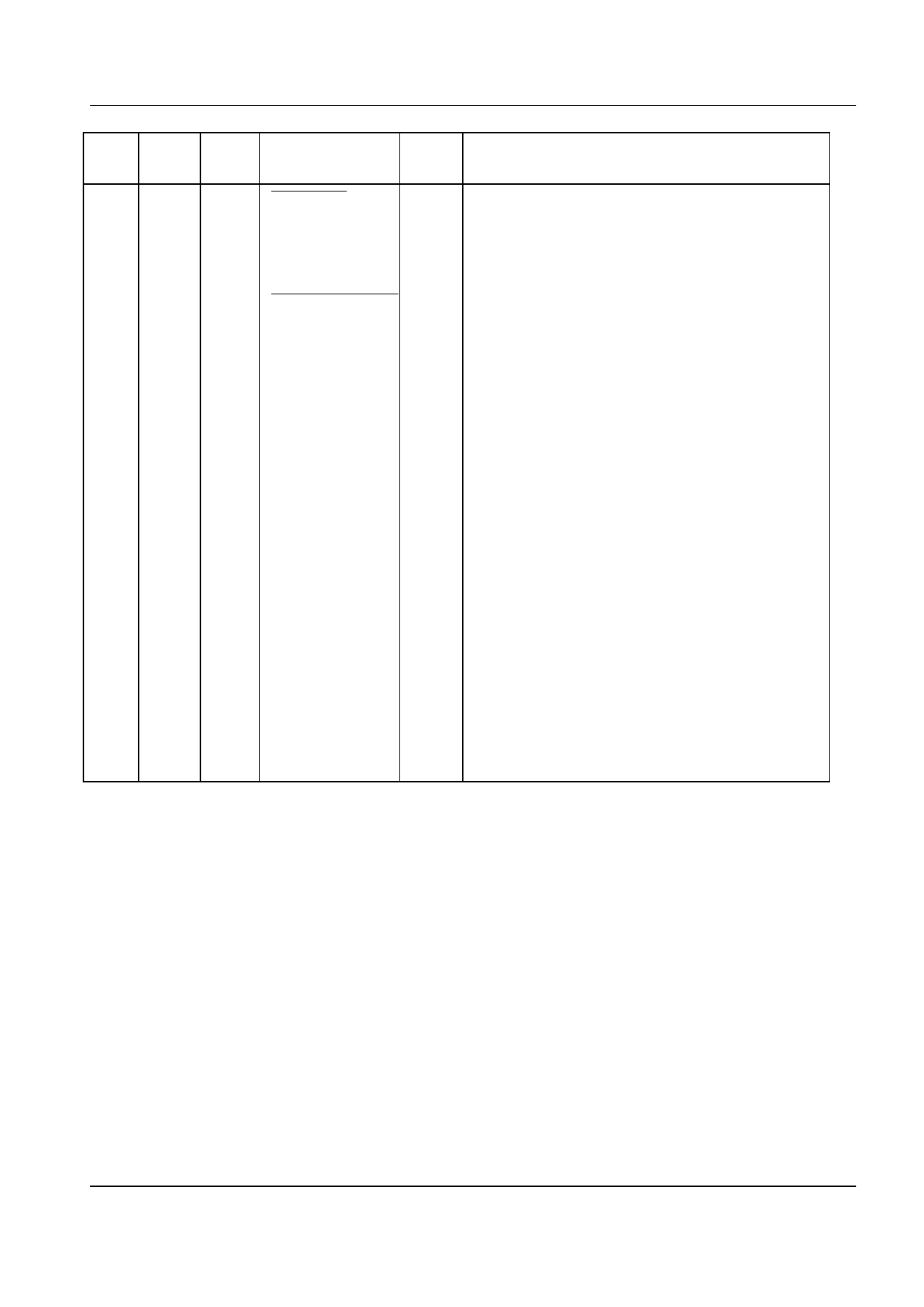
Signal Name
Powersave
Type
Input
N/C
Decoder Force Idle input
Decoder Input
Decoder Data
Clock
input
input/
output
Algorithm
input
Clock Mode 2
input
Clock Mode 1
input
VDD
power
Description
A logic '0' at this pin puts most parts of the codec
into a quiescent, non-operational state. When at a
logical '1', the codec operates normally. Internal 1
MΩ pull-up.
No Connection
A logic '0' at this pin gates a ‘0101...’ pattern
internally to the decoder so that the Decoder
Output goes to VDD/2. When this pin is a logical
'1' the decoder operates as normal. Internal 1MΩ
pull-up.
The received digital signal input. Internal 1 MΩ
pull-up.
A logic I/O port. External decode clock input or
internal data clock output. Clock frequency is
dependent upon Clock Mode 1 and 2 inputs and
Xtal frequency. Note: No internal pull-up is
provided. See Table 3.
A logic '1' at this pin sets this device for a 3-bit
companding algorithm. A logical '0' sets a 4-bit
companding algorithm. Internal 1 MΩ pull-up.
Clock rates refer to f = 1.024MHz Xtal/Clock input.
During internal operation the data clock
frequencies are available at these ports for
external circuit synchronization. Independent or
common data rate inputs to Encode and Decode
data clock ports may be employed in the External
Clocks mode. Internal 1MΩ pull-ups. See Table 3.
Positive Supply. A single 3.0V to 5.5V supply is
required. This pin should be externally decoupled
to VSS by capacitor C5.
© 2000 Consumer Microcircuits Limited
5
CMX639/2
Share Link: 