UPC1934 查看數據表(PDF) - NEC => Renesas Technology
零件编号
产品描述 (功能)
比赛名单
UPC1934 Datasheet PDF : 20 Pages
| |||
µ PC1934
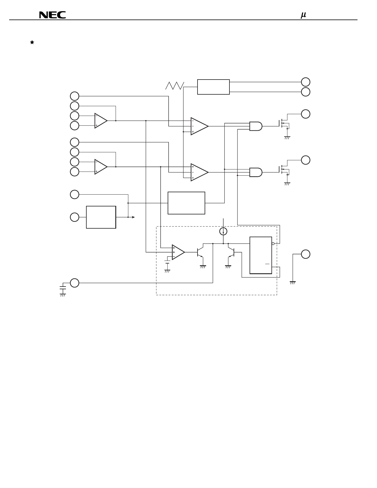
2. CONFIGURATION AND OPERATION OF EACH BLOCK
Figure 2-1 Block Diagram
DTC1 6
FB1 5
II1 4
IN1 3
DTC2 11
FB2 12
II2 13
IN2 14
Error amplifier
Error amplifier
VREF 16
VCC 9
Reference
voltage
section
DLY
15
CDLY
Oscillation
section
PWM
comparator
Output
section
PWM
comparator
Under voltage
lock-out
section
Output
section
SCP
comparator
Q1
Q2
0.63 V
SQ
Q
Timer latch for
short-circuit
protection section
2 RT
1 CT
7 OUT1
10 OUT2
8 GND
2.1 Reference Voltage Generator
The reference voltage generator is comprised of a band-gap reference circuit, and outputs a temperature-compensated
reference voltage (2.1 V). The reference voltage can be used as the power supply for internal circuits, or as a reference
voltage, and can also be accessed externally via the VREF pin (pin 16).
2.2 Oscillator
The oscillator self-oscillates if a timing resistor is attached to the RT pin (pin 2). Also, the oscillator outputs the
symmetrical triangular waveform if a timing capacitor is attached to the CT pin (pin 1). This oscillator waveform is input to
the non-inverted input pins of the two PWM comparators to determine the oscillation frequency.
10
Data Sheet G13567EJ3V0DS00
Share Link: 