UPD750064(A) 查看數據表(PDF) - NEC => Renesas Technology
零件编号
产品描述 (功能)
比赛名单
UPD750064(A) Datasheet PDF : 82 Pages
| |||
µPD750064, 750066, 750068, 750064(A), 750066(A), 750068(A)
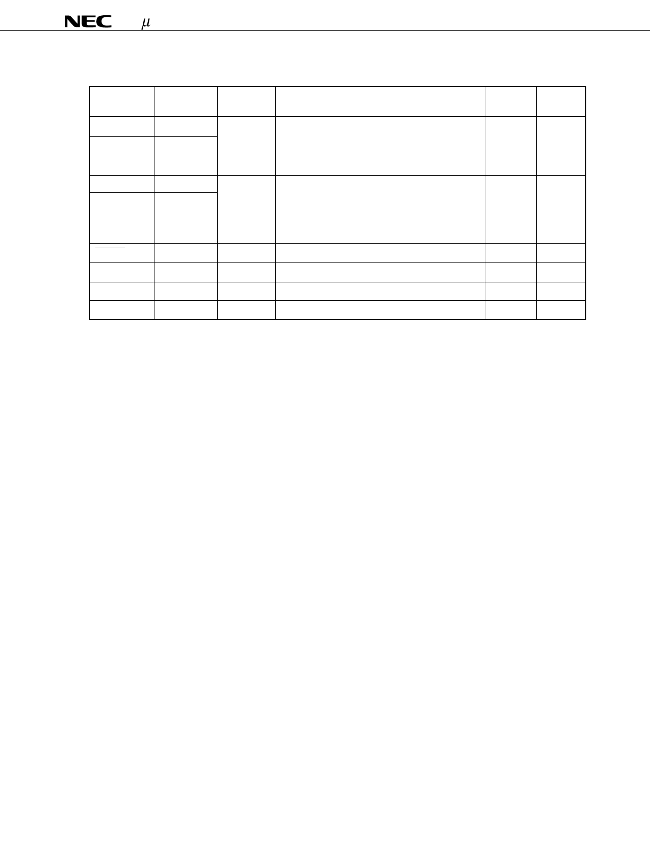
3.2 Non-port Pins (2/2)
Pin Name
X1
X2
XT1
XT2
RESET
IC
VDD
VSS
Input/Output
Input
–
Input
–
Input
–
–
–
Alternate
Function
–
–
–
–
–
–
Function
I/O Circuit
After Reset
TypeNote
Crystal/ceramic connection pin for the main system
–
–
clock oscillation. When inputting the external
clock, input the external clock to pin X1, and the
inverted phase of the external clock to pin X2.
Crystal connection pin for the subsystem clock
–
–
oscillation. When the external clock is used, input
the external clock to pin XT1, and the inverted
phase of the external clock to pin XT2. Pin XT1 can
be used as a 1-bit input (test) pin.
System reset input (low-level active)
–
<B>
Internally connected. Connect directly to VDD.
–
–
Positive power supply
–
–
Ground potential
–
–
Note Circuit types enclosed in brackets indicate the Schmitt trigger input.
Data Sheet U10165EJ2V0DS00
11
Share Link: 