W149(2000) 查看數據表(PDF) - Cypress Semiconductor
零件编号
产品描述 (功能)
比赛名单
W149 Datasheet PDF : 14 Pages
| |||
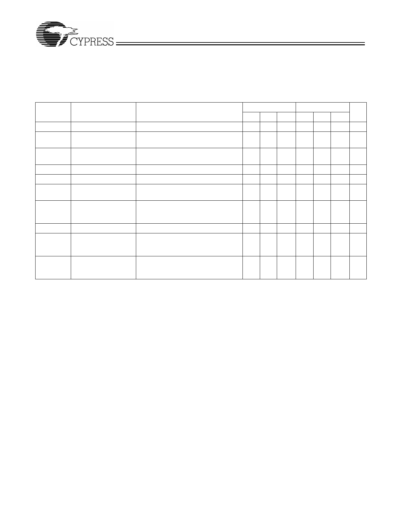
W149
SDRAM Clock Outputs, SDRAM, SDRAM0:11 (Lump Capacitance Test Load = 30 pF)
CPU = 66.6 MHz
Parameter
Description
Test Condition/Comments Min. Typ. Max.
tP
Period
tH
High Time
Measured on rising edge at 1.5V 30
Duration of clock cycle above 2.4V, 5.6
at min. sdge rate (1.5 V/ns)
tL
Low Time
Duration of clock cycle below 0.4V, 5.3
at min. sdge rate (1.5 V/ns)
tR
Output Rise Edge Measured from 0.4V to 2.4V
1.5
4
Rate
tF
Output Fall Edge
Measured from 2.4V to 0.4V
1.5
4
Rate
tPLH
Prop Delay LH
Input edge rate faster than 1 V/ns 1
5
tPHL
Prop Delay HL
Input edge rate faster than 1 V/ns 1
5
tD
Duty Cycle
Measured on rising and falling
45
55
edge at 1.5V, at min. sdge rate
(1.5 V/ns)
tJC
Jitter, Cycle-to-Cycle Measured on rising edge at 1.5V.
250
Maximum difference of cycle time
between two adjacent cycles.
tSK
Output Skew
Measured on rising edge at 1.5V
250
tO
CPU to PCI Clock Covers all CPU/PCI outputs. Mea- 1.5
4
Skew
sured on rising edge at 1.5V. CPU
leads PCI output.
fST
Frequency
Assumes full supply voltage
3
Stabilization from
reached within 1 ms from
Power-up (cold start) power-up. Short cycles exist prior
to frequency stabilization.
Zo
AC Output
Average value during switching
30
Impedance
transition. Used for determining
series termination value.
CPU = 100 MHz
Min. Typ. Max. Unit
30
ns
3.3
ns
3.1
ns
1.5
4 V/ns
1.5
4 V/ns
1
5 ns
1
5 ns
45
55 %
250 ps
250 ps
1.5
4 ns
3 ms
30
Ω
11
Share Link: 