W149H 查看數據表(PDF) - Cypress Semiconductor
零件编号
产品描述 (功能)
比赛名单
W149H Datasheet PDF : 16 Pages
| |||
W149
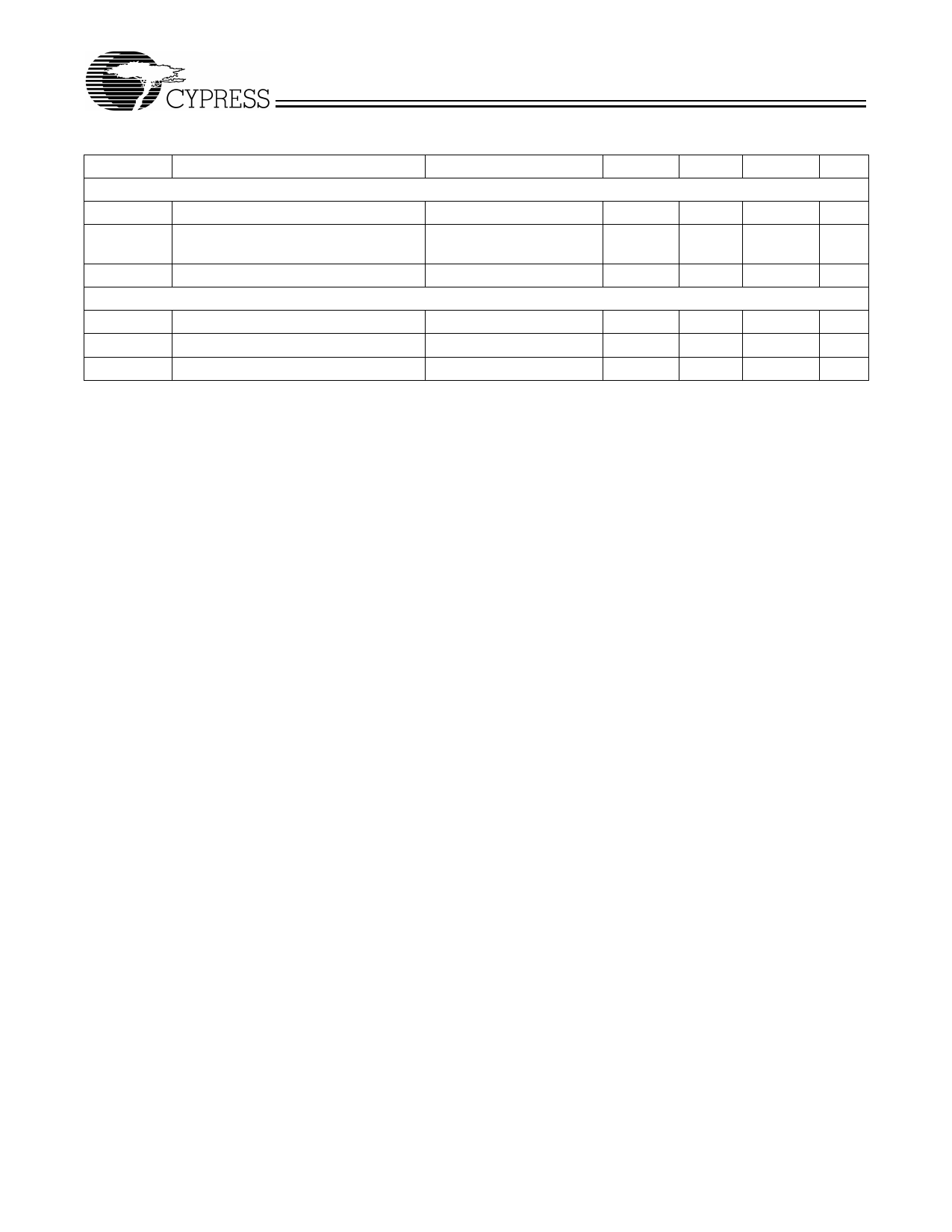
DC Electrical Characteristics: (continued) TA = 0°C to +70°C; VDDQ3 = 3.3V±5%; VDDQ2 = 2.5V±5%
Parameter
Description
Test Condition
Min.
Typ.
Max. Unit
Crystal Oscillator
VTH
X1 Input threshold Voltage[7]
CLOAD
Load Capacitance, Imposed on
External Crystal[8]
CIN,X1
X1 Input Capacitance[9]
Pin Capacitance/Inductance
VDDQ3 = 3.3V
Pin X2 unconnected
1.65
V
14
pF
28
pF
CIN
Input Pin Capacitance
Except X1 and X2
5
pF
COUT
Output Pin Capacitance
6
pF
LIN
Input Pin Inductance
7
nH
Notes:
7. X1 input threshold voltage (typical) is VDDQ3/2.
8. The W149 contains an internal crystal load capacitor between pin X1 and ground and another between pin X2 and ground. Total load placed on crystal is
14 pF; this includes typical stray capacitance of short PCB traces to crystal.
9. X1 input capacitance is applicable when driving X1 with an external clock source (X2 is left unconnected).
Document #: 38-07176 Rev. *A
Page 10 of 16
Share Link: 