W155 查看數據表(PDF) - Cypress Semiconductor
零件编号
产品描述 (功能)
比赛名单
W155 Datasheet PDF : 6 Pages
| |||
W155
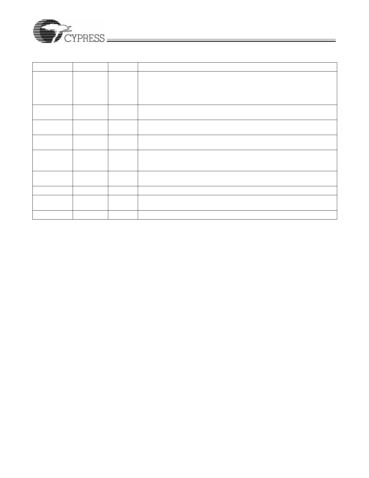
Pin Definitions
Pin Name
Pin No.
USBCLK/
14
SS%
SYSCLK
FS0:3
SSON#
X1
X2
TEST
VDD
GND
12
10, 8, 7, 5
9
2
3
16
1, 6, 15
4, 11, 13
Pin Type
I/O
O
I
I
I
I
I
P
G
Pin Description
USB Clock Output/Modulation Width Selection Input: When an input; if spread
spectrum feature is enabled, this pin is used to select the amount of frequency
variation on the SYSCLK output (see Table 2). Wider variations result in greater
peak EMI reduction. When an output: supplies a non-spread 48-MHz signal for
USB support.
System Clock Output: Frequency is selected per Table 1. Spread spectrum fea-
ture is controlled by pins 9 & 14.
Frequency Select Pins: These pins set the frequency of the signal provided at
the SYSCLK output.
Spread Spectrum Control (active LOW): Pulling this input signal HIGH turns the
internal modulating waveform off. This pin has an internal pull-down resistor.
Crystal Connection or External Reference Frequency Input: This pin has dual
functions. It can be used as either an external crystal connection, or as an external
reference frequency input.
Crystal Connection: If using an external reference, this pin must be left uncon-
nected.
Test Mode: For normal operation, tie this pin to ground.
Power Connection: Connected to either 3.3V or 5.0V power supply. All VDD pins
must be the same voltage level.
Ground Connection: Connect to the common system ground plane.
2
Share Link: 