W163 查看數據表(PDF) - Cypress Semiconductor
零件编号
产品描述 (功能)
比赛名单
W163 Datasheet PDF : 5 Pages
| |||
W163
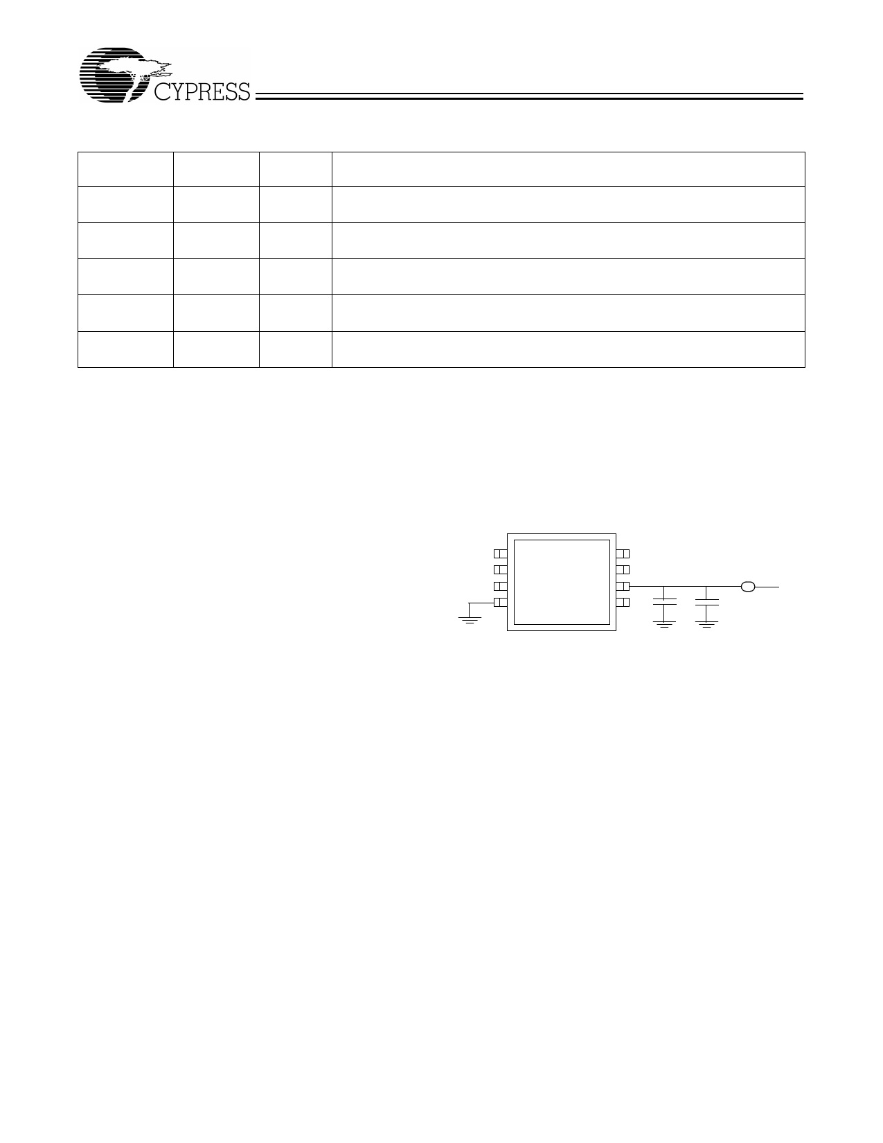
Pin Definitions
Pin Name
REF
Q0:3
QFB
VDD
GND
Pin No.
1
2, 3, 5, 7
8
6
4
Pin
Type
I
O
O
P
P
Pin Description
Reference Input: The output signals Q0:3 will be synchronized to this signal
unless the device is programmed to bypass the PLL.
Outputs: These signals will be synchronous and of equal frequency to the signal
input at pin 1.
Feedback Output: This output signal does not vary from signals Q0:3 in function,
but is noted as the signal used to establish the propagation delay of nearly 0.
Power Connections: Connect to 3.3V. Use ferrite beads to help reduce noise
for optimal jitter performance.
Ground Connections: Connect all grounds to the common system ground
plane.
Overview
The W163 products are five-output zero delay buffers. A
Phase-Locked Loop (PLL) is used to take a time-varying signal
and provide five copies of that same signal out. The internal
feedback to the PLL provides outputs in phase with the refer-
ence inputs.
which may cause problems in systems requiring synchroniza-
tion.
For more details on Spread Spectrum timing technology,
please see the Cypress Application note titled, “EMI Suppres-
sion Techniques with Spread Spectrum Frequency Timing
Generator (SSFTG) ICs.”
Schematic
Spread Aware
Many systems being designed now utilize a technology called
Spread Spectrum Frequency Timing Generation. Cypress has
been one of the pioneers of SSFTG development, and we de-
signed this product so as not to filter off the Spread Spectrum
feature of the Reference input, assuming it exists. When a
zero delay buffer is not designed to pass the SS feature
through, the result is a significant amount of tracking skew
REF
Q0
Q1
GND
QFB
Q3
VDD
Q2
Ferrite
Bead
0.1 µF 10 µF
VDD
Document #: 38-07149 Rev. *A
Page 2 of 5
Share Link: 