W164(1999) 查看數據表(PDF) - Cypress Semiconductor
零件编号
产品描述 (功能)
比赛名单
W164 Datasheet PDF : 11 Pages
| |||
W164
Writing Data Bytes
Each bit in the data bytes controls a particular device function
except for the “reserved” bits, which must be written as a logic
0. Bits are written MSB (most significant bit) first, which is bit
7. Table 4 gives the bit formats for registers located in Data
Bytes 3–6.
Table 5 details additional frequency selections that are avail-
able through the serial data interface.
Table 6 details the select functions for Byte 3, bits 1 and 0.
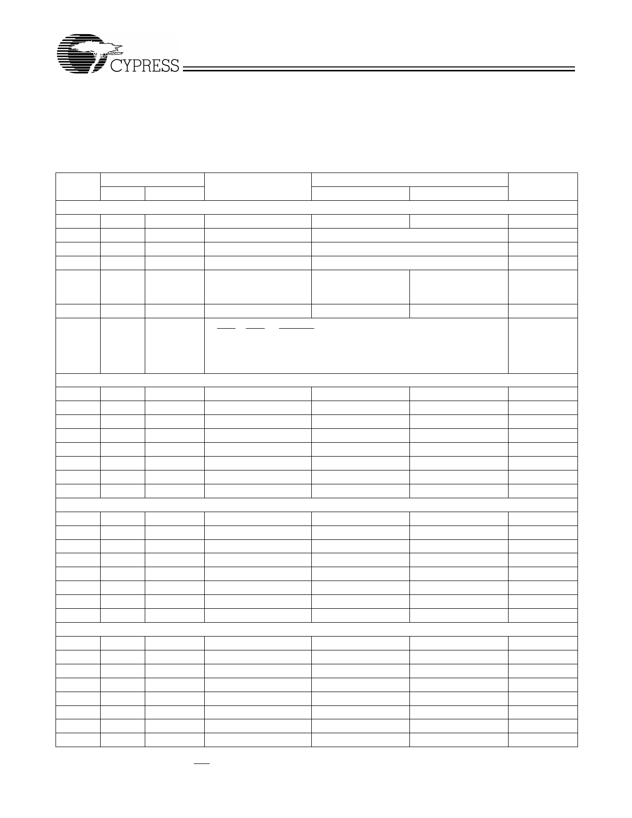
Table 4. Data Bytes 3–6 Serial Configuration Map
Affected Pin
Bit Control
Bit(s) Pin No. Pin Name
Control Function
0
1
Data Byte 3
7
--
--
SEL_3
--
--
6
--
--
SEL_2
Refer to Table 5
5
--
--
SEL_1
Refer to Table 5
4
--
--
SEL_0
Refer to Table 5
3
--
--
Frequency Table
Selection
Frequency Controlled Frequency Controlled
by external SEL100/ by BYT3 SEL_(3:0)
66# pin Table 1
Table 5
2
--
--
(Reserved)
--
--
1–0
--
--
Bit 1 Bit 0 Function (See Table 6 for function details)
0
0 Normal Operation
0
1 Test Mode
1
0 Spread Spectrum on
1
1 All Outputs Three-stated
Data Byte 4
7
--
--
(Reserved)
--
--
6
14
24/48MHz Clock output Disable
Low
Active
5
--
--
(Reserved)
--
--
4
--
--
(Reserved)
--
--
3
--
--
(Reserved)
--
--
2
21
CPU1 Clock Output Disable
Low
Active
1
--
--
(Reserved)
--
--
0
22
CPU0 Clock Output Disable
Low
Active
Data Byte 5
7
4
PCI_F Clock Output Disable
Low
Active
6
11
PCI6
Clock Output Disable
Low
Active
5
10
PCI5
Clock Output Disable
Low
Active
4
-
--
(Reserved)
--
--
3
8
PCI4
Clock Output Disable
Low
Active
2
7
PCI3
Clock Output Disable
Low
Active
1
6
PCI2
Clock Output Disable
Low
Active
0
5
PCI1
Clock Output Disable
Low
Active
Data Byte 6
7
--
--
(Reserved)
--
--
6
--
--
(Reserved)
--
--
5
24
IOAPIC Clock Output Disable
Low
Active
4
--
--
(Reserved)
--
--
3
--
--
(Reserved)
--
--
2
--
--
(Reserved)
--
--
1
27
REF2X Clock Output Disable
Low
Active
0
27
REF2X Clock Output Disable
Low
Active
Note:
1. Both Bits 0 and 1 of Byte 6 in Table 4 must be programmed as the same value.
Default
0
0
0
0
0
0
00
0
1
0
0
0
1
0
1
1
1
1
0
1
1
1
1
0
0
1
0
0
0
1[1]
1[1]
5
Share Link: 