W167B 查看數據表(PDF) - Cypress Semiconductor
零件编号
产品描述 (功能)
比赛名单
W167B Datasheet PDF : 18 Pages
| |||
PRELIMINARY
W167B
Signaling Requirements
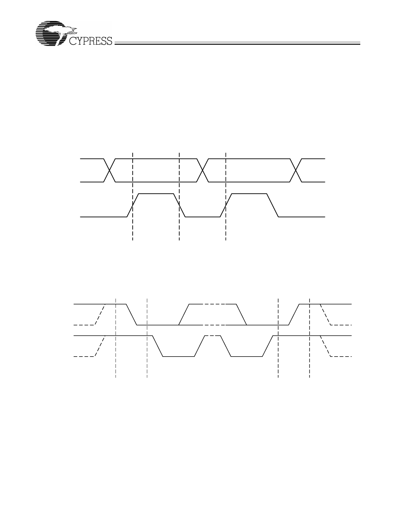
As shown in Figure 6, valid data bits are defined as stable logic
0 or 1 condition on the data line during a clock HIGH (logic 1)
pulse. A transitioning data line during a clock HIGH pulse may
be interpreted as a start or stop pulse (it will be interpreted as
a start or stop pulse if the start/stop timing parameters are
met).
A write sequence is initiated by a “start bit” as shown in Figure
7. A “stop bit” signifies that a transmission has ended.
As stated previously, the W167B sends an “acknowledge”
pulse after receiving eight data bits in each byte as shown in
Figure 8.
Sending Data to the W167B
The device accepts data once it has detected a valid start bit
and address byte sequence. Device functionality is changed
upon the receipt of each data bit (registers are not double buff-
ered). Partial transmission is allowed meaning that a transmis-
sion can be truncated as soon as the desired data bits are
transmitted (remaining registers will be unmodified). Transmis-
sion is truncated with either a stop bit or new start bit (restart
condition).
SDATA
SCLOCK
Valid
Data
Bit
Change
of Data Allowed
Figure 6. Serial Data Bus Valid Data Bit
SDATA
SCLOCK
Start
Bit
Stop
Bit
Figure 7. Serial Data Bus Start and Stop Bit
11
Share Link: 