W149 查看數據表(PDF) - SpectraLinear Inc
零件编号
产品描述 (功能)
比赛名单
W149 Datasheet PDF : 15 Pages
| |||
W149
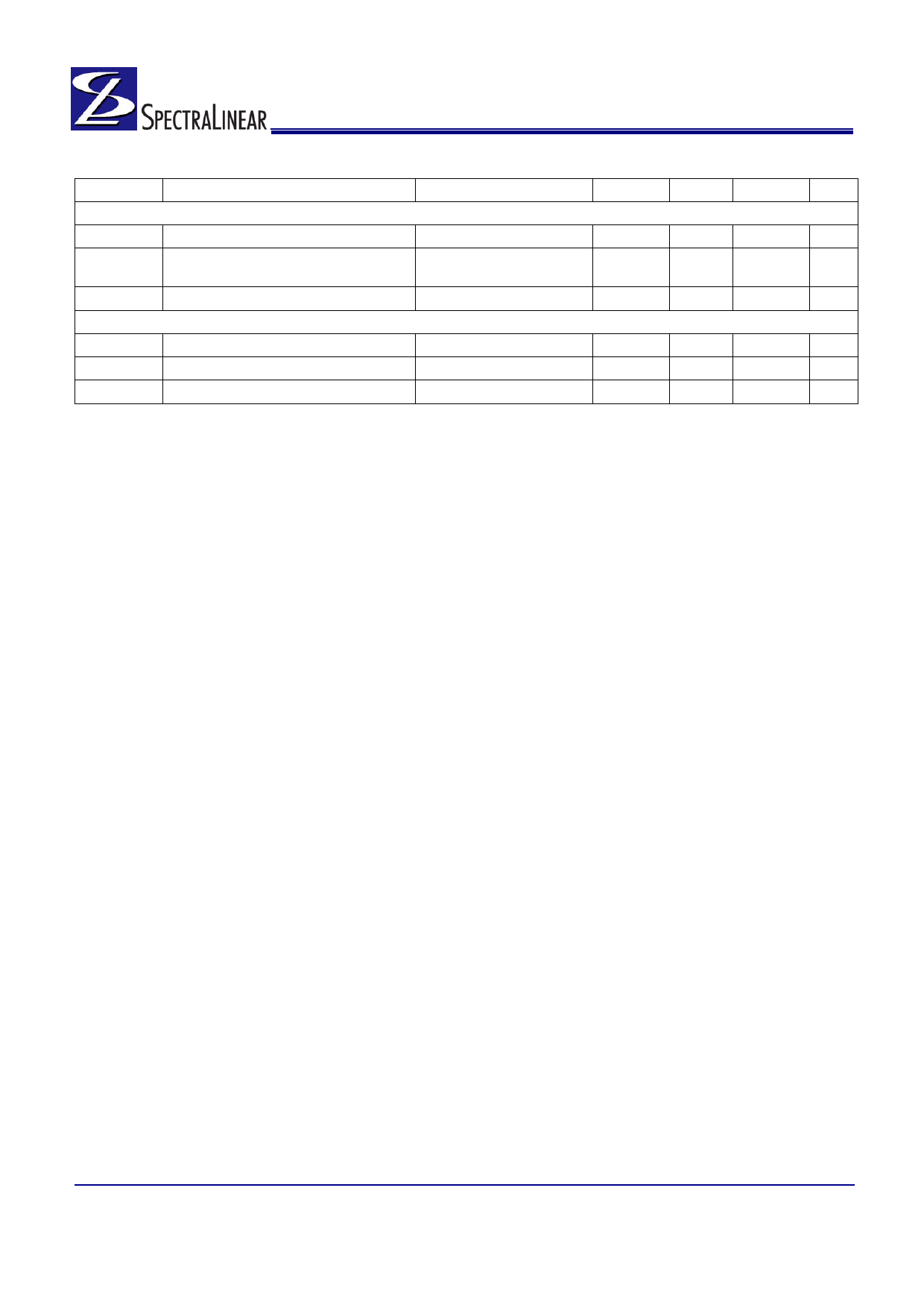
DC Electrical Characteristics: (continued) TA = 0°C to +70°C; VDDQ3 = 3.3V±5%; VDDQ2 = 2.5V±5%
Parameter
Description
Test Condition
Min.
Typ.
Max. Unit
Crystal Oscillator
VTH
X1 Input threshold Voltage[7]
CLOAD
Load Capacitance, Imposed on
External Crystal[8]
CIN,X1
X1 Input Capacitance[9]
Pin Capacitance/Inductance
VDDQ3 = 3.3V
Pin X2 unconnected
1.65
V
14
pF
28
pF
CIN
Input Pin Capacitance
Except X1 and X2
5
pF
COUT
Output Pin Capacitance
6
pF
LIN
Input Pin Inductance
7
nH
Notes:
7. X1 input threshold voltage (typical) is VDDQ3/2.
8. The W149 contains an internal crystal load capacitor between pin X1 and ground and another between pin X2 and ground. Total load placed on crystal is 14 pF;
this includes typical stray capacitance of short PCB traces to crystal.
9. X1 input capacitance is applicable when driving X1 with an external clock source (X2 is left unconnected).
Rev 1.0, November 21, 2006
Page 10 of 15
Share Link: 