W742C814 查看數據表(PDF) - Winbond
零件编号
产品描述 (功能)
比赛名单
W742C814 Datasheet PDF : 46 Pages
| |||
W742C814
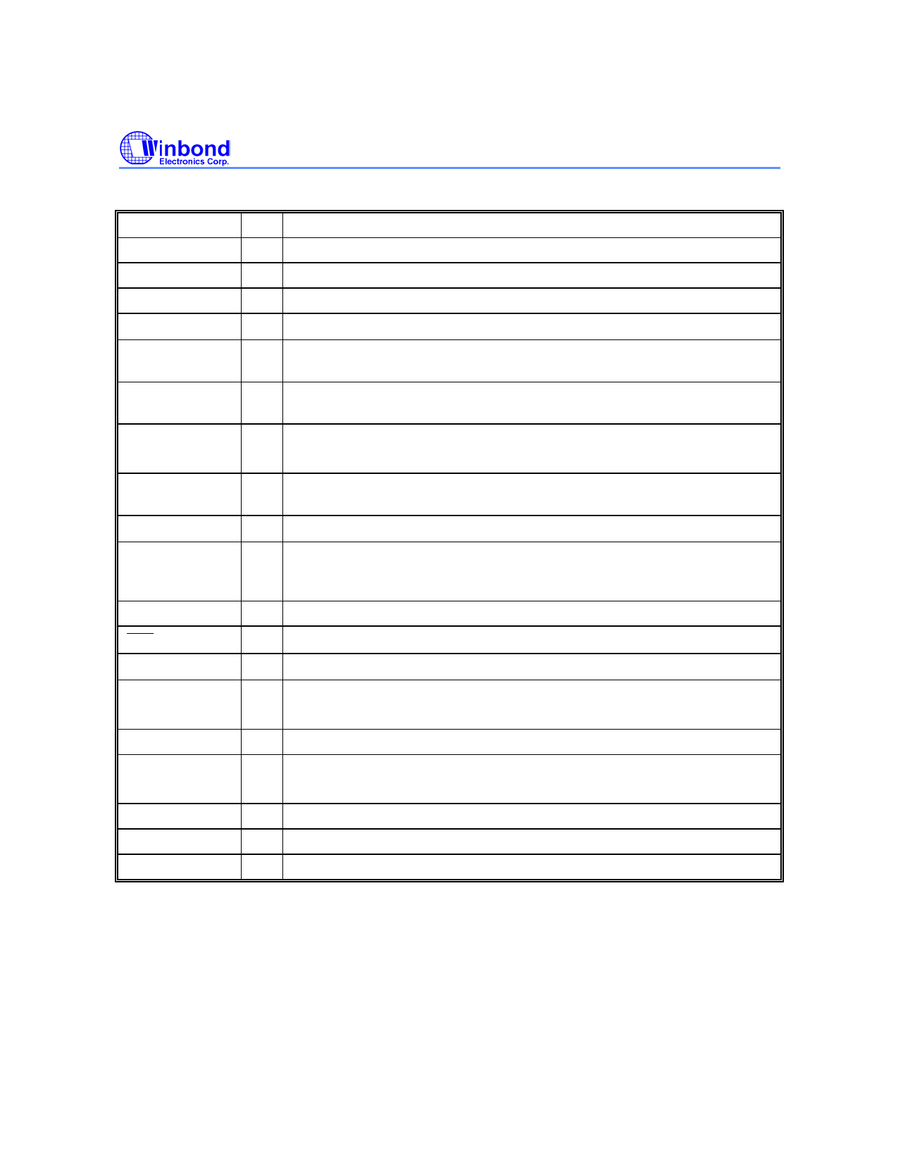
4. PIN DESCRIPTION
SYMBOL
XIN
XOUT
VF
VXXF
RA0 − RA3
RB0 − RB3
RC0 − RC3
RD0 − RD3
RE0 − RE3
MFP
DTMF
I/O
FUNCTION
I Input pin for 32.768 Hz oscillator. Connected to 32.768 KHz crystal only.
O Output pin for 32.768 Hz oscillator. Connected to 32.768 KHz crystal only.
I Low pass filter for PLL circuit. Connected capacitor to VSS.
I Regulator for PLL circuit. Connected capacitor (10 µF) to VSS.
I/O
Input/Output port.
Input/output mode specified by port mode 1 register (PM1).
I/O
Input/Output port.
Input/output mode specified by port mode 2 register (PM2).
4-bit port for input only.
I
Each pin has an independent interrupt capability.
I/O
Input/Output port.
Input/output mode specified by port mode 5 register (PM5).
O Output port only. With high sink current capacity for the LED application.
Output pin only.
O
This pin can output modulating or nonmodulating frequency, or Timer 1
specified frequency. It can be selected by bit 0 of BUZCR (BUZCR.0).
O This pin can output dual-tone multifrequency signal for dialling.
RES
SEG0 − SEG31
COM0 − COM3
DH1, DH2
VDD1
VDD2
TEST1, TEST2
VDD
VSS
I System reset pin.
O LCD segment output pins.
LCD common signal output pins.
O
The LCD alternating frequency can be selected by code option.
I Connection terminals for voltage doubler (halver) capacitor.
Positive (+) supply voltage terminal.
I
Refer to Functional Description.
I For IC testing used, User don’t care these pin.
I Positive power supply (+).
I NEGATIVE POWER SUPPLY (-).
Publication Release Date: February 12, 2003
-5-
Revision A2
Share Link: 