LTC1690I 查看數據表(PDF) - Linear Technology
零件编号
产品描述 (功能)
比赛名单
LTC1690I Datasheet PDF : 12 Pages
| |||
LTC1690
DC ELECTRICAL CHARACTERISTICS The q denotes the specifications which apply over the full operating
temperature range, otherwise specifications are at TA = 25°C. VCC = 5V ±5% (Notes 2, 3)
SYMBOL PARAMETER
VOH
VOL
RIN
ICC
IOSD1
IOSD2
IOZ
IOSR
tPLH
tPHL
tSKEW
tr, tf
tPLH
tPHL
tSKD
fMAX
Receiver Output High Voltage
Receiver Output Low Voltage
Receiver Input Resistance
Supply Current
Driver Short-Circuit Current, VOUT = HIGH
Driver Short-Circuit Current, VOUT = LOW
Driver Three-State Current (Y, Z)
Receiver Short-Circuit Current
Driver Input to Output, Figure 3, Figure 4
Driver Input to Output, Figure 3, Figure 4
Driver Output to Output, Figure 3, Figure 4
Driver Rise or Fall Time, Figure 3, Figure 4
Receiver Input to Output, Figure 3, Figure 5
Receiver Input to Output, Figure 3, Figure 5
|tPLH – tPHL|, Differential Receiver Skew, Figure 3, Figure 5
Maximum Data Rate, Figure 3, Figure 5
CONDITIONS
IO = – 4mA, VID = 200mV
IO = 4mA, VID = – 200mV
–7V ≤ VCM ≤ 12V
No Load
–7V ≤ VO ≤ 10V
–7V ≤ VO ≤ 10V
–7V ≤ VO ≤ 10V, VCC = 0V
0V ≤ VO ≤ VCC
RDIFF = 54Ω, CL1 = CL2 = 100pF
RDIFF = 54Ω, CL1 = CL2 = 100pF
RDIFF = 54Ω, CL1 = CL2 = 100pF
RDIFF = 54Ω, CL1 = CL2 = 100pF
RDIFF = 54Ω, CL1 = CL2 = 100pF
RDIFF = 54Ω, CL1 = CL2 = 100pF
RDIFF = 54Ω, CL1 = CL2 = 100pF
RDIFF = 54Ω, CL1 = CL2 = 100pF
MIN
q 3.5
q
q 12
q
35
35
q
q7
q 10
q 10
q
q2
q 30
q 30
q5
TYP MAX UNITS
V
0.4
V
22
kΩ
260 600
µA
250
mA
250
mA
5
200
µA
85
mA
22.5
60
ns
25
60
ns
2.5
15
ns
13
40
ns
94
160
ns
89
160
ns
5
ns
Mbps
Note 1: Absolute Maximum Ratings are those values beyond which the life
of the device may be impaired.
Note 2: All currents into device pins are positive; all currents out of device
pins are negative. All voltages are referenced to device ground unless
otherwise specified.
Note 3: All typicals are given for VCC = 5V and TA = 25°C.
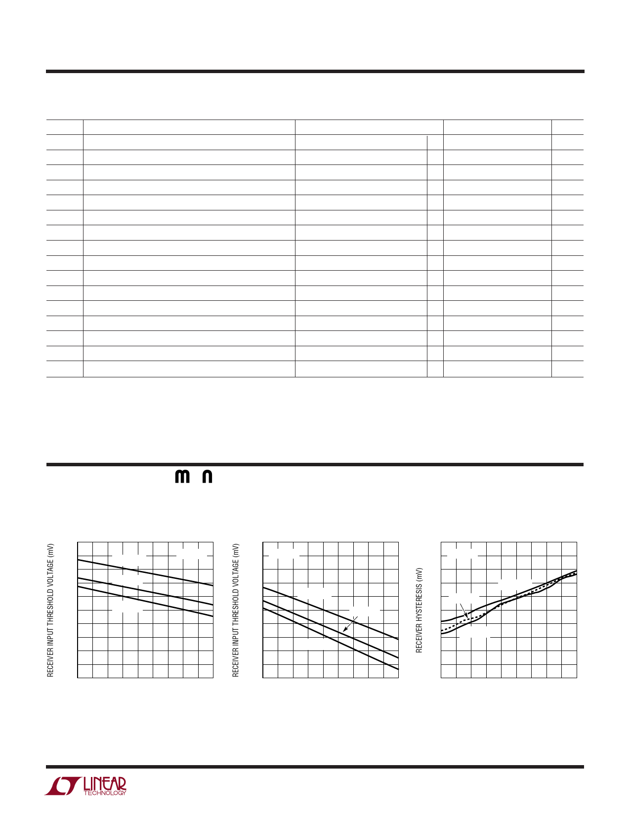
TYPICAL PERFOR A CE CHARACTERISTICS
Receiver Input Threshold Voltage
(Output High) vs Temperature
0
–20
VCM = 12V
VCC = 5V
–40
–60
VCM = 0V
–80
–100
VCM = –7V
–120
–140
–160
–180
–200
–55 –35 –15 5 25 45 65 85 105 125
TEMPERATURE (°C)
1690 G01
Receiver Input Threshold Voltage
(Output Low) vs Temperature
0
–20 VCC = 5V
–40
–60
–80
VCM = 12V
–100
–120
VCM = 0V
–140
–160
VCM = –7V
–180
–200
–55 –35 –15 5 25 45 65 85 105 125
TEMPERATURE (°C)
1690 G02
Receiver Hysteresis vs
Temperature
100
90 VCC = 5V
80
70
60 VCM = 0V
50
VCM = 12V
40
30
VCM = –7V
20
10
0
–55 –35 –15 5 25 45 65 85 105 125
TEMPERATURE (°C)
1690 G03
3
Share Link: 